fclifton
Newbie level 1
contact cleaning current
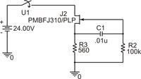
I have inherited a circuit we use as part of an input circuit to which relay contacts are connected. The circuit is designed to allow an initial high current (which cleans the relay contacts) and then settle to a non-zero steady state current. The circuit works, but I need to figure out how to determine the steady state current mathmatically. I realize that because of the JFET properties the steady state current will have a range of possible values.
Things I understand about how the circuit works:
When the input has power applied (relay contacts close) the JFET is "on" and saturated, because Vgs = 0, because
As power is applied, the initial voltage on both R3 and R2 will be the same, via C1, and it will be about Vr3 = Idss * R3.
As C1 charges, Vr2 will decrease roughly as the time constant of R2*C1 until it reaches 0V. The result is that over time, Vgs becomes more negative. Once Vr2 = Vg = 0, whatever Id and Vds (thus Vr3) are, they will remain at that point, and the steady state current will be = Vgs/R3.
What I can't figure out is how to mathematically describe what the value of that steady state current will be.
The JFET datasheet is attached.
