Continue to Site

Welcome to EDAboard.com

Welcome to our site! EDAboard.com is an international Electronics Discussion Forum focused on EDA software, circuits, schematics, books, theory, papers, asic, pld, 8051, DSP, Network, RF, Analog Design, PCB, Service Manuals... and a whole lot more! To participate you need to register. Registration is free. Click here to register now.

is this mosfet snubber scheme correct ?

Status
Not open for further replies.

anotherbrick

Full Member level 4
Joined
Jan 10, 2009
Messages
217
Helped
1
Reputation
2
Reaction score
1
Trophy points
1,298
Location
Istanbul , Turkey
Activity points
3,143
hello dear forum

I want to add snubber to my mosfet H bridge

the DC link voltage is 300 VDC

and the H bridge circuit works as inverter producing 30 - 100 Hz alternating square wave

the values of components is not true I will use 100 nF and 1 K and UF4007

I want to ask if the following scheme is correct ?

thank you
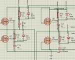
mehmet1.JPG
 

Not exactly.
The snubber, as shown, will control the rate of rise of the voltage across Vds. Excessive rate of rise produces ringing in single ended converters.
If your dead time between the upper and lower Mosfets is long enough to produce ringing, there could be some value to this. Otherwise, when the opposite Mosfet turns on, that consideration is not relevant.
 
the driving of the mosfets is as follows

the left_up and right_down turns on with %10 - %90 duty
and they turn off and in the next cycle
the right_up and left_down turns on with %10 - %90 duty

when the left_up is ON the left_down is OFF and
when the right_up is ON the right_down is OFF

can you comment about the above scheme with this driving please ?
thank you
 

At 100 Hz, and 90% duty cycle, you have 1/2 millisec deadtime between transitions.

In that case, your snubber will help to dampen high frequency ringing.

100 nF may be too much. I would start with 1 nF, and measure with a scope the Vds. Experiment with different values.
You will require a X10 scope probe which has been properly compensated and a scope with at least 40 Mhz bandwidth.
 
Hi,

If you want to protect the fets for overvoltage, then the snubber circuit may not be a good solution. Use fast recovery diods across D-S of each fet.

More common are snubber circuits with scr and triacs to avoid ringing an reducing dU/dt and dI/dt.

Good luck
 

hello dear forum members

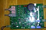
I am having trouble with my circuit
this is simply an inverter changing the frequency and the duty of the 220 V
board.JPG

the output frequency is changed between 25 - 105 Hz

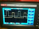
here you can see the output voltage
there is an unwanted ringing at the turn off of mosfets
smallduty.JPG

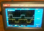
when I increase the duty of the output
the ringing gets bigger and bigger

( here I connect a 750 W 220-24 trafo as the load )

biggerduty.JPG

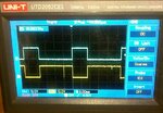
this is the gate signal of one of the upper mosfets the dusy is at the minimum

uppergate.JPG

this is both of the lower mosfet gates
duty is a little bigger

lowergates.JPG

I suspect the snubber circuit
please look at my snubber circuit scheme in the original post

the capacitor is 100 nF resistor is 1 K
and the diode is UF4007

please advice what can I do with my circuit to function correctly

becouse at my first trial with a real load 3 minutes later all of the mosfets blown up
 

I assume that you are driving a steel-cored transformer.

Those transformers have an enormous amount of energy stored as magnetizing current. That spike you are seeing is the magnetizing current being returned back as the core flux resets.

I built 60Hz inverters in the mid-1980s using steel core transformers and that is exactly how I remember the waveforms.

What you have to do is add a tertiary winding to reset the transformer's core during the deadtime.

Another set of Mosfets, which are driven only when the main Mosfets ARE NOT BEING driven, dumps that energy into a resistor, or if you are clever enough, back into the battery.

You have also mentioned that you are driving the transformer at various frequencies...are you aware of the volt-second relationship in transformers? If you exceed that at the lowest frequencies, the transformer will saturate.
On the other hand, unless you are using a very good magnetic steel grade, at the higher frequencies the core losses may be excessive and the transformer will overheat.
 
As a first point, it's a completely bad idea to use RCD snubbers for H-bridges, whatever the R and C values are. They are good for single ended or transformer push-pull output stages. In H-bridges, theý cause high peak currents and additional switching losses.

Secondly, the ringing is produced by free-wheeling the H-bridge, as already pointed out by schmitt trigger. I don't see a reasonable purpose of this operation mode, instead I would operate the H-bridge in synchronous push-pull mode with a short (10 to 100 ns range) dead time between high and low side on-time.

Small RC snubbers might be used if high frequent (MHz) ringing occurs, but it's probably not needed in a H-bridge with good layout and low inductance bus capacitors.
 
Hi,

as said before. what you call "ringing" is caused by the transformer´s inductivity.
This pulls back energy to your DC supply.

And here is the point. Do you have lowESR capacitors in addition with ceramic capacitors near the drain of the upper FET?
They must have a very low impedance connection to your GND plane. I hope you have one. Also the source of the lower FETs need the low impedance connection to this GND plane.
The pulse itself must not harm your FETs, but the increased voltage - even very short pulses - on drain may destroy it.


... instead I would operate the H-bridge in synchronous push-pull mode with a short (10 to 100 ns range) dead time between high and low side on-time...

So th operation should be sometihing like that:
Code:
Left; right side bridge
low ; low ; 
high; low ; 
low ; low ;
low ; high;
repeating.
low means: the lower FET is active, the upper is inactive
high means the upper fet is active and the lower is inactive.
mind: there is no high Z state (exept during dead time)

the high time of the right side must perfectly match the high time of the left side. to avoid DC and therfore saturation of the core.

You picture shows a low side controlled PWM. I recommend here a high side controlled PWM. means that both sides are low when not active.
With that you can drive both sides low as long as you want. But you can not drive high for a long time because of bootstrap capacitor discharge.

Hope this helps
Klaus
 
The oscillation shown in post #6 has rather low energy, transformer main inductance with off-state MOSFET output capacitance. The voltage is safely clamped by the FET substrate diodes, no risk to damage anything.
 
first of all thank you everyone who answered

The oscillation shown in post #6 has rather low energy, transformer main inductance with off-state MOSFET output capacitance. The voltage is safely clamped by the FET substrate diodes, no risk to damage anything.

in particular I want ask something about above comment

if there is "no risk to damage anything"
why can my mosfets ( all four ) be blown up ?

I am using my circuit with a vibrator tank ( below photo )

ecc.jpg

my customer said the circuit operated 5 minutes good
then there was a smoke and stopped working

in addition I want say that if I increase duty of the square wave ( mosfets ON ) the ringing ( return of trafo magnetizing current ) seen in the pictures combines with the square wave of "opposite" mosfets and becomes one single square wave

thank you
 

Hi,

in addition I want say that if I increase duty of the square wave ( mosfets ON ) the ringing ( return of trafo magnetizing current ) seen in the pictures combines with the square wave of "opposite" mosfets and becomes one single square wave

Yes, this is because you leave the bridge OPEN / HiZ when not activated. It is the energy stored in the magnetic field and in the moving mass of your vibrator tank.

I recommend NOT to leavethe bridges OPEN / HiZ. You now switch it:
HiZ - positive - HiZ - negative

I´d try:
0V - positive - 0V - negative ( forcing 0V instead of HiZ)

Klaus
 
hello all forum members

I changed the software a little bit according your previous comments

here the up_right and down_left gate signals

upright_downleft.JPG

here up and down left

up_and_down_left.JPG

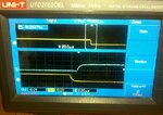
and here the 2 uSec deadtime

deadtime.JPG

of this operation mode, instead I would operate the H-bridge in synchronous push-pull mode with a short (10 to 100 ns range) dead time between high and low side on-time.

as you can see there is gate capacitor charging at least 1 uSec - I can make deadtime as low as 1 uSec

is there a danger of having the deadtime greater than 100 nSec ?

thank you
 

In a bridge, the deadtime should be enough to prevent top and bottom Mosfet cross-conduction, which would lead to high shoot-thru currents.

In other words, the MosFet that is turning off, should already be completely off by the time the Mosfet that is turning on reaches the Miller plateau.
 
Status
Not open for further replies.

Part and Inventory Search

Welcome to EDABoard.com

Sponsor

Back
Top