Continue to Site

Welcome to EDAboard.com

Welcome to our site! EDAboard.com is an international Electronics Discussion Forum focused on EDA software, circuits, schematics, books, theory, papers, asic, pld, 8051, DSP, Network, RF, Analog Design, PCB, Service Manuals... and a whole lot more! To participate you need to register. Registration is free. Click here to register now.

Interfacing PCI9054 in burst mode,need help!

Status
Not open for further replies.

janlee

Newbie level 5
Joined
Sep 23, 2006
Messages
10
Helped
0
Reputation
0
Reaction score
0
Trophy points
1,281
Activity points
1,365
pci9054

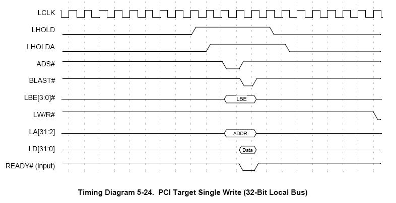
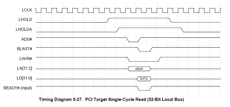
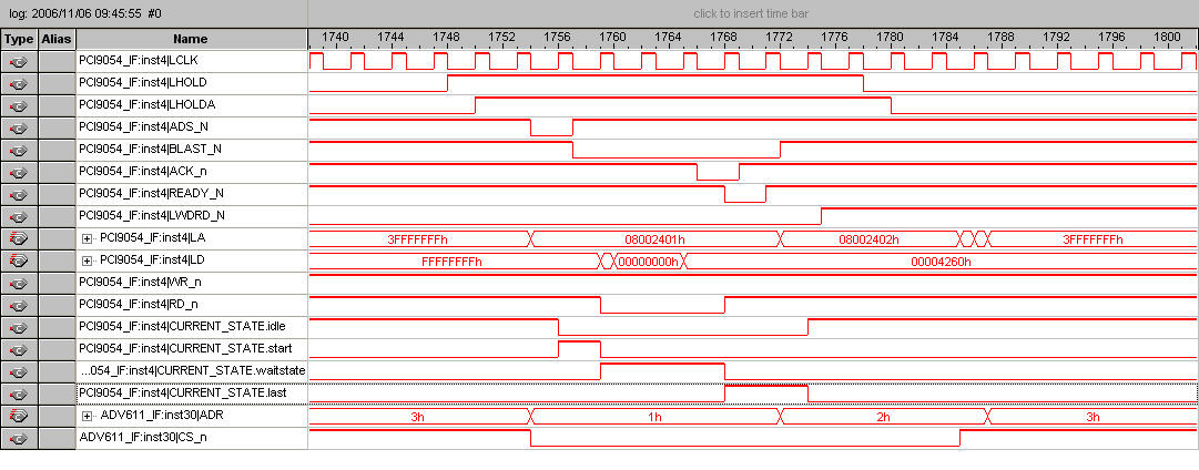
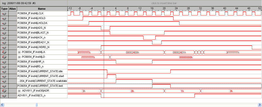
In my project I use PCI9054 "C Mode" to control FPGA and other peripherals.Acturally PCI9054 acts as local bus master and PCI target.

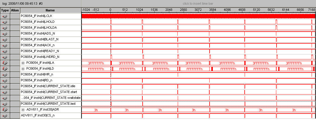
I successfully realize the signal cycle 32 bits read & write.But it quite slow,the interval between two continous read or write is more than 12 us.To control register in the FPGA is not a problem,but to transfer large block of data in real time it is not accecptable.

Now my question is how to configure the PCI9054 to lanch a burst transfer via PLX's funcions(I wonder which function I can use) ,and how to modify my code to adapt this transfer.

Many appreciations.

Code:
--------------------------------------------- 
--Module      : PCI9054 interface Module 
--File        : PCI9054_IF.vhd 
--Library     : IEEE; 
--Description : PCI9054 interface controller 
--Simulator   : Modelsim 5.8/WindowsXP 
--Synthesizer : 
--Author      : 
--Created     : 06/07/2006 
--Last update : 25/07/2006 
--------------------------------------------- 

library ieee; 
use ieee.std_logic_1164.all; 
use ieee.std_logic_unsigned.all; 
use ieee.std_logic_arith.all; 

entity PCI9054_IF is 
port( 
      RST_N : in std_logic; 
      LCLK : in std_logic; 
      LHOLD : in std_logic; 
      ADS_N : in std_logic; 
      BLAST_N : in std_logic; 
      LWDRD_N : in std_logic; 
      LA : in std_logic_vector(31 downto 2); 
      LD : inout std_logic_vector(31 downto 0); 
      LHOLDA : out std_logic; 
      READY_N : out std_logic; 
      ACK_n : in std_logic; 
      WR_n : out std_logic; 
      RD_n : out std_logic 
             
   ); 
end PCI9054_IF; 

architecture RTL of PCI9054_IF is 
type STATE_TYPE is (IDLE,START,WAITSTATE,LAST); 
signal CURRENT_STATE,NEXT_STATE : STATE_TYPE; 
signal iready_n : std_logic; 

signal iwr_n,ird_n : std_logic; 
signal iaddr : std_logic_vector(31 downto 2); 

begin 
    
    
   -- 
   --Grant for local bus request 
   process(LCLK) 
   begin 
      if (LCLK'event and LCLK = '1') then 
         if LHOLD = '1' then 
            LHOLDA <= LHOLD; 
         else 
            LHOLDA <= '0'; 
         end if; 
      end if; 
   end process; 
    
   --State Machine Transition 
   process(LCLK) 
   begin 
      if RST_n = '0' then 
         CURRENT_STATE <= IDLE; 
      elsif(LCLK'event and LCLK = '1') then 
         CURRENT_STATE <= NEXT_STATE; 
           
         if CURRENT_STATE = IDLE and ADS_N = '0'then 
            iaddr <= LA; 
         end if; 

         READY_n <= iready_n ;      
          
      end if; 
   end process; 
    
   --State Machine 
   process(CURRENT_STATE,ADS_N,LWDRD_N,BLAST_N,ACK_n) 
   begin 
      NEXT_STATE <= CURRENT_STATE; 
      case CURRENT_STATE is 
         when IDLE => 
            RD_n <= '1'; 
            WR_n <= '1'; 
            iready_n <= '1'; 
            if ADS_N = '0' then 
               NEXT_STATE <= START; 
            else 
               NEXT_STATE <= IDLE; 
            end if; 
          
         when START => 
            RD_n <= '1'; 
            WR_n <= '1'; 
            iready_n <= '1'; 
            if BLAST_N = '0' then 
               NEXT_STATE <= WAITSTATE; 
            else 
               NEXT_STATE <= START; 
            end if; 
          
         when WAITSTATE => 
            RD_n <= LWDRD_N; 
            WR_n <= not LWDRD_N; 
             
            if iaddr(31 downto 4) = B"0010_0000_0000_0000_1001_0000_0000"   then 
               if ACK_n = '0' then 
                  NEXT_STATE <= LAST; 
                  iready_n <= '0'; 
               else 
                  NEXT_STATE <= WAITSTATE; 
                  iready_n <= '1';    
               end if; 
            else 
               NEXT_STATE <= LAST; 
               iready_n <= '0';       
            end if; 
             
          
         when LAST => 
            RD_n <= '1'; 
            WR_n <= '1'; 
            iready_n <= '1'; 
            if ADS_N = '1' and BLAST_N = '1' then 
               NEXT_STATE <= IDLE; 
            elsif ADS_N = '0' then 
               NEXT_STATE <= START; 
            else 
               NEXT_STATE <= LAST; 
            end if; 
          
         when others => 
            RD_n <= '1'; 
            WR_n <= '1'; 
            iready_n <= '1'; 
            NEXT_STATE <= IDLE; 
      end case; 
   end process; 
    
    
end RTL;
 

pci 9054 problem

I think that 12us for a single rd/wr cycle is too much. I'm worked few years ago with PCI9054 and this acces time was about 100ns (i'm configured this time to 100ns for proper acces to local SRAM).

I think that your PCI9054 are not configured properly.

From your vhd code I understood that your PCI9054 act as PCI master. Can you tell me which timing diagrams (from databook) are used to implement the vhd code?
 

how to access the pci9054 using fpga

Thanks for ur replay! :D

U may misunderstand that I said the intervals of continous read or write cycle is 12us,rather than the singal read or write cycle itself . The singal cycle is quite fast it consumes 4~5 LCLK,I wonder what the OP system do when in the interval of continous singal read and write cycle.

Please help me!

88_1162764595.JPG


69_1162764638.JPG
 

pci9054 local bus+timing diagram

The 12us delay even between rd/wr cycles is too much.
What are the value of LCLK? And PCI to local registers are proper configured?

Anyway, i suggest to assert iready_n signal on the following clock after ADS_N signal is asserted (if your FPGA can accept data)
 

plx write main configuration registers

The LCLK is 25MHz,I do assert Ready_n after ADS_n,but I use address to differenciate the 2 peripherals(FPGA's registers and ADV611).FPGA's internal registers doesn't have ACK_n,ADV611 has its ACK_n.

I wonder PLX's functions is the only way to configure PCI9054 into burst mode.But I didn't know how to do .

54_1162856073.jpg

4_1162856101.jpg

65_1162856128.jpg
 

pci9054 local control signal timing diagram

I wonder PLX's functions is the only way to configure PCI9054 into burst mode.But I didn't know how to do

You can use the same PLX functions to read all PLX registers. You should control this registers for proper PLX operation. Maybe your PLX registers are not configured to use READY# signal...

The next quote is from data book:
If READY# mode is disabled, the external READY#
input signal has no effect on wait states for a Local
access. Wait states between Data cycles are asserted
internally by a wait state counter. The wait state
counter is initialized with its Configuration register
value at the start of each data access.
If READY# mode is enabled, it has no effect until the
wait state counter reaches 0. READY# then controls
the number of additional wait states.
BTERM# input is not sampled until the wait state
counter reaches 0. BTERM# overrides READY# when
BTERM# is enabled and asserted.
 

Did you finally have it working?
Can you post your code please.
I'm trying to interface with PLX 9056
 

Re: pci9054

Did you finally have it working?
Can you post your code please.
I'm trying to interface with PLX 9054
my email is m.tajalipour@gmail.com
please help.
thanks.
 

So do I
I am working in interface with a pci 9030. I studied the project a few months ago, and I need help to continue.
Please if someone like to work together or someone have some information i would be very grateful.
contact us jcastillo@rfranco.com
 

Status
Not open for further replies.

Part and Inventory Search

Welcome to EDABoard.com

Sponsor

Back
Top