Continue to Site

Welcome to EDAboard.com

Welcome to our site! EDAboard.com is an international Electronics Discussion Forum focused on EDA software, circuits, schematics, books, theory, papers, asic, pld, 8051, DSP, Network, RF, Analog Design, PCB, Service Manuals... and a whole lot more! To participate you need to register. Registration is free. Click here to register now.

Integrate low voltage signal

Status
Not open for further replies.

orienteraren

Junior Member level 1
Joined
Dec 9, 2009
Messages
16
Helped
0
Reputation
0
Reaction score
0
Trophy points
1,281
Activity points
1,436
Hi!

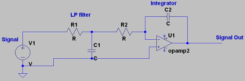
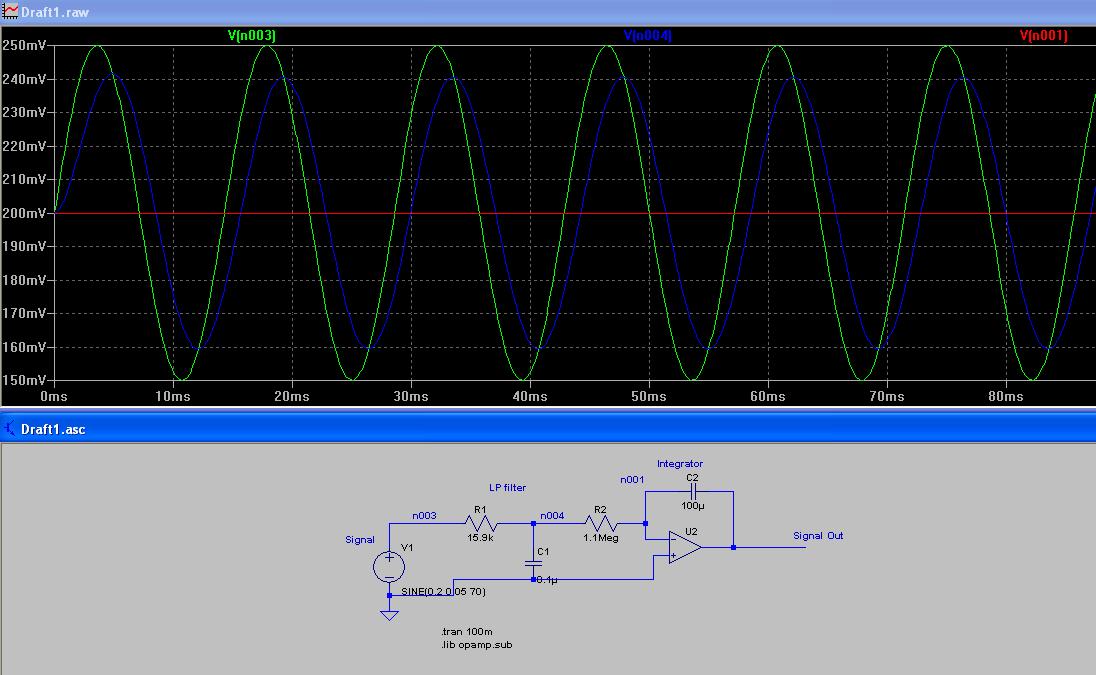
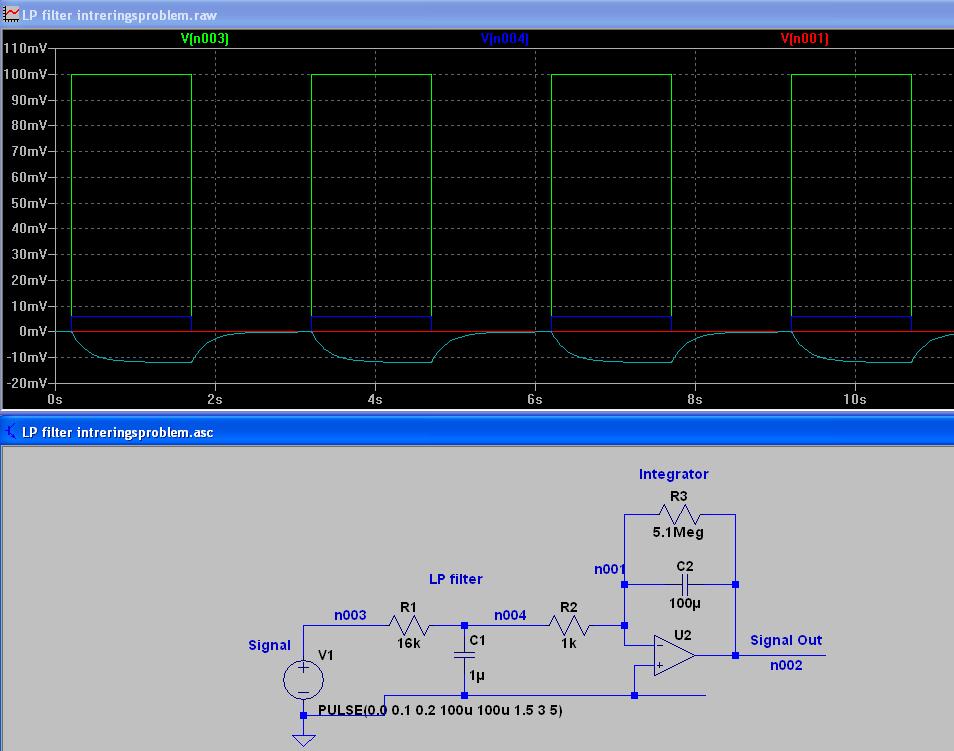
I have a low voltage signal (range +/- 50 mV) after I run it through a simple LP filter. I now want to integrate the signal using a larger capacitor but if I connect the signal to the - input on the OP amp I get 0V, both on the input and on the output. I suppose this is a fundamental think in my design, any suggestions?

Best Regards

Fredrik
 

I now want to integrate the signal using a larger capacitor but if I connect the signal to the - input on the OP amp I get 0V, both on the input and on the output.

It is absolutely not clear what your intention is. Please, in your own interest, show us your circuit.
 
Here is the circuit, the signal is output from a sensor that I want to run through a LP filter and then integrate. I do have a resetswitch over the capacitor for reseting it.

Here is the circuit:
 

As a trivial explanation for the output stuck at zero, did you open the reset switch? The circuit is basically correct as shown, assuming you have a bipolar supply according to the OP specification and are using suitable dimensioned components, considering real OP parameters as input current and input resistance.
 

The switch is open, already tried that. After simulating the circuit in LTspice (I added correct values and replacedthe OPamp with another model) I do get the same issue as in real life, zero voltage after the second resistor. I must be doing some logical error that I cannot see. I´m attaching my new circuit and simulaitons reults.

In this simulation I have a sine wave of DC=0.2V and an amplitude of 0.05V.


Regards

Fredrik
 

Some comments to your circuit:
* I cannot see any switch
* The RC lowpass is loaded by R2 - did you consider R2 in the low pass design?
* Each opamp integrator needs a resistor across the integrating capacitor because of necessary dc feedback (fixed opamp bias point) - unless the circuit is part of an overall feedback loop.
* After "the second resistor" (I guess you mean R2) the voltage must be always app. 0 volts (virtual ground principle at the opamp input).
*Try to understand the opamp integrator principle in detail (articles, textbooks).
 
LvW is right in all his points. Just to try to make it a bit more clearer, if there is no DC path in the feedback, then any DC signal at the input, no matter how small (offsets etc) will charge your capacitor, leading finally the opamp to saturation and the output to the rail.
Also, when you simulate a transient usually the simulation starts from the DC operating point. That is, if your input has a dc component, then at DC the output will necessarily hit one of the rails (in dc analysis the capacitor effectively doesn't exist, so the opamp is effectively a comparator!). So when the transient analysis starts, even if your DC at the input is exactly zero (or better, equal to the offset of the opamp), you will still see a zero output. You can avoid this by resetting the capacitor when your simulation starts, or setting an initial condition on the capacitor.
 
Thanks for the comments.

- No there is no switchin the circuit diagram but I do have a manual switch across the capacitor in the real circuit.

- In what way does R2 affect the low pass properties? The voltage drop over R1 and then C1 to GND should handle all of the filtering I thoght?

- I realize that the simulation I published is misleading since I do not have a DC-offset in the real circuit, I just put it in here to make it clearer but it backfired and made it less clear. Anyhow, my sensor gives me 0 DC voltage offset.

- "So when the transient analysis starts, even if your DC at the input is exactly zero (or better, equal to the offset of the opamp), you will still see a zero output. You can avoid this by resetting the capacitor when your simulation starts, or setting an initial condition on the capacitor. " I have now redesign the circuit and added a reistor over the capacitor. The circuit does work while simulating (havn´t had time to test it for real yet) but why is the potential at node n001 zero (ok a few nV) while I do get a nice output signal?

Attached the new circuit with a pulse input.


Regards Fredrik
 

- In what way does R2 affect the low pass properties? The voltage drop over R1 and then C1 to GND should handle all of the filtering I thoght?


Because of the virtual ground principle the inverting opamp input voltage is nearly zero (in reality: some nV). Therefore, R2 is in parallel to C1 and influences the corner frequency of the RC lowpass (R1 and R2 have to be considered in parallel).

I have now redesign the circuit and added a reistor over the capacitor. The circuit does work while simulating (havn´t had time to test it for real yet) but why is the potential at node n001 zero (ok a few nV) while I do get a nice output signal?


Do you really consider the output signal as "nice"? It is a typical lowpass response, which is not surprising since the additional R3 in paralell to C2 makes a nice lowpass. However, up to now, I was of the opinion you are trying to design an integrating device.
Question: What is the frequency of the signal to be integrated?
Advice: Recalculate the circuit and select an active lowpass (opamp with R2, R3, C2) with a corner frequency which is well below your actual signal frequency. Perform some ac analyses and verify if the signal frequency is in the integrating range (magnitude drop of app. -20dB/dec and phase app. 90 deg).
 

- The input impedance of the integrator (which is R2) effectively comes in parallel to the LPF capacitor, forming a voltage divider. This is the reason that your signal at node004 is much smaller than your input signal (effectively by R2/(R1+R2)).
- The signal at node n001 SHOULD be almost zero, because of the negative feednack of the opamp that creates a virtual ground!
- Your output is not really "nice". If the integrator was designed properly you should be getting a ramp for a pulse input. The fact that your output actually "sees" your input and responds to it makes me wonder if the values of the elements you show on the picture are the same ones you are simulating for. 100uF in parallel to 5.1MEG give a time constant of about 500 secs, so your output should have been adapting much more slower! Also, the dc gain of the integrator doesnt look right.

edit: sorry if there is some overlap with what LvW says. Wrote it at the same time, but thought you might gain from two explanations of the same thing...
 

If you calculate the expectable output voltage of the integrator with sine input, it's in a few µV order of magnitude. So I think, as far as it can be determined from the shown waveform, the output magnitude is pretty O.K. You may want to adjust the amplitude scaling if you want to see more.
 

Thanks for helpful answers!

After reading your replies and considering a textbook I now think I got the koncept of virtual ground, thank you!


Yes, I am trying to create an integrating circuit. The signal that I want to integrate is rather sketchy and noisy, explaining the filtering I want to do. The signal contains frequencies between (roughly) 20-140 Hz but the main part is in the 65-70 Hz range.

Does this mean that I should design the corner frequency to be at 7 Hz? And why not the freq. Im looking for? Chosing a lower freq would mean that I attenuate everything above 7 Hz (in this case) which means that I´d attenuate my real signal, right?

kgl_13gr: Yes, what you see is the simulated circuit.

Regards

Fredrik
 

Does this mean that I should design the corner frequency to be at 7 Hz? And why not the freq. Im looking for? Chosing a lower freq would mean that I attenuate everything above 7 Hz (in this case) which means that I´d attenuate my real signal, right?


Yes, in principle you are right. If the signal range to be integrated is app. around 70 Hz, the corner frequency of the active lowpass should be not higher than app. 5 Hz. However, this does not mean that you attenuate the signals because your active circuit has gain! But, on the other hand, you need rather large element values for this design; this may cause some offset problems.
 

Status
Not open for further replies.

Similar threads

Part and Inventory Search

Welcome to EDABoard.com

Sponsor

Back
Top