Continue to Site

Welcome to EDAboard.com

Welcome to our site! EDAboard.com is an international Electronics Discussion Forum focused on EDA software, circuits, schematics, books, theory, papers, asic, pld, 8051, DSP, Network, RF, Analog Design, PCB, Service Manuals... and a whole lot more! To participate you need to register. Registration is free. Click here to register now.

Input common range and capacitive coupling

Status
Not open for further replies.

Junus2012

Advanced Member level 5
Joined
Jan 9, 2012
Messages
1,552
Helped
47
Reputation
98
Reaction score
53
Trophy points
1,328
Location
Italy
Activity points
15,235
Hello,

A common issue of the three op-amp instrumentation amplifier (in-amp) is the relationship between the required gain the common mode voltage of the input signal.

However, if we capacitively couple the input signal or even transformer coupling with a common mode voltage fixed to the middle of the in-amp then we must suffer from this issue. A circuit to perform this one is given below
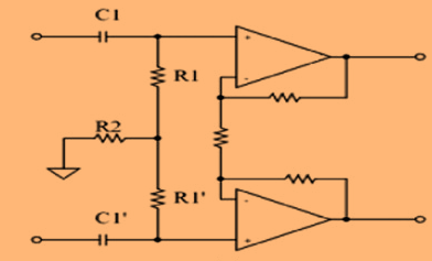
Capture.PNG


The -3dB frequency of the coupling circuit is set by 1/(2*pi*R1*C1) and can be down do few Hertz.

My question is, if this solution is simple, why designers complain on the input common-mode voltage issue, basically when the DC is blocked at the input (decoupled), the amplifier behave just like an ideal rail to rail input stage.

Thank you
Best Regards
 
This :

"The output diff amp ’s function in the three opamp IA is to provide common mode rejection.
The input amplifiers may provide gain 2 but no CMR; A1 and A 2 are both non-inverting
operational amp lifiers so any CM V at the inputs is amplified by + 1 and appears at their
respective outputs. CMR is provided solely by the output difference amplifier— we’ll look at this
later."

So you are setting the CM Bias at input, and those R's and C's have to be matched, keeping in
mind the IA is laser trimmed in output AMP to achieve CMR, AC and DC.

Is this what you are referring to ?


Regards, Dana.
 
The question isn't completely clear. Post #1 refers to limited common mode range and doesn't address specifically common mode rejection.

Common mode range is a problem of DC coupled differential amplifiers. If AC coupling is an option, you don't worry about common mode range.
 
CM range is limited when the sum of AC and DC common mode force
input stage into non linear operation.

Or so I think.....:)


Regards, Dana.
 
Hi,

I´m a bit confused.
In post#1 you talk about "three OPAMP" whereas I see just 2 OPAMPs. So let´s focus on this shown circuit.

To avoid confusion we should differ between
* INA_input (= left side of the capacitors) and
* OPAMP_input (right side of the capacitors)

Although the capacitor attenuates the DC .... still common mode input voltage range of the OPAMP is valid.
Example: if the positive supply is 5V and the upper CMIVR is limited to VCC-1.5V then the input (of each OPAMP input) is limited to +3.5V.

From input view (which also means CMIVR view) both shown OPAMPs work independently ...as if they were used as two independently working non inverting buffers.

Until here I see no "special case" for an INA circuit with respect to the OPAMP inputs.

But there is a difference for the OPAMP outputs: here the
* INA_diff_input is amplified with high gain (OPAMP2_out - OPAMP1_out)
* INA_comm_input is amplified with gain = 0 (OPAMP2_out - OPAMP1_out)
But this has nothing to do with the CMIVR of the shown circit (as long as we don´t discuss the - not shown - second stage of an INA)

*****
I agree with Dana regarding the second stage...

Klaus
 
Last edited:
Dear friends,

Thank you all very much for your reply,

I want to clear my post since as FvM is say it is becoming confusing,

Let me post this circuit below without going to the detail of the instrumentation amplifier

TMR.jpg


As you can see the inputs to the InAmp is capacitively coupled,

As FvM commented: "Common mode range is a problem of DC coupled differential amplifiers. If AC coupling is an option, you don't worry about common mode range."

That was indeed my question, so if it is easy like this way why we pay constraint to design rail to rail amplifiers?
The only tradeoff I see from the AC coupling is sacrefying the DC processing, which is by any way not lovely component since it couples both sensor offset and the supply disturbance as a differential components to the InAmp.

I want to discuss with you the consequence of the AC coupling on the performance of the InAmp, and weather it is recommended procedure to follow every time.

I believe that your talking will lead to discuss about the coupling circuit mismatching effect to the CMRR of the amplifier, but in the same time using resistor components with low tolearnces of 1 % and capacitors with tolearnces of 5 % should be enough to preserve the CMRR of the amplifier.


Thank you all once again
Regards
 

Here is a tool that might be useful for you (can be configed AC)


The output amp CMRR, discussing not range but rejection, is unaffected by the input
structure, but overall CM present at output of IA potentially higher because your tolerances
at input of components generate, potentially, more CM presented at input to deal with.

Regards, Dana.
 
Hi,

I guess I never did AC coupling when I used an INA ... because I was interested in the DC. So for me AC coupling never was an option.
So from my point of view AC coupling is no solution.

On one point I agree with FvM: "If AC coupling is an option..." the emphasis is on "IF" ...
On the other hand: This is only true if the common mode voltage is DC. But if the common mode voltage is AC, then even DC coupling does not help.
Example: current measurement on a PWM driven BLDC motor coil.

weather it is recommended procedure to follow every time.
Surely not. It depends on the application.

using resistor components with low tolearnces of 1 % and capacitors with tolearnces of 5 % should be enough to preserve the CMRR of the amplifier.
I can´t generally agree. It also depends on the application.

And
 
Last edited:
Dear friends,

Thank you all for your nice explanation and for the useful links you shared with me. It was very useful.

I agrre that depending on the application, if the sensor is not DC varying then AC coupling is a good option to consider as I read by the materials.
For example, sensor bridges can have an offset output voltage that will be understood by the amplifier as a differential voltage which gives an output error.
Secondly and in some application like for example for measuring the biomedical signal from human body, usually the common mode voltage at the output of sensor electrode are far away from the input common mode range of the InAmp.

In the latter two cases the AC coupling is becoming necessary.

The consequence of the AC coupling components as per my reading becomes like this:
1.The value of the resistors introduces noise added to the InAmp circuit
2. The value of the resistors together with the input bias current of the InAmp differential pair creat an offset voltage depending. Hence those resistors should not be large (R1, and R1' from my first post)
3. The mismatch between R1 and R1' degrade the CMRR of the InAmp, that is why R2 is used to reduce this effect with a value of R2 >>R1.


To share my reading with you as for your interest,

I found this useful paper:


The last but not the least, the author in the following paper argued that the input impedance of the InAmp will be reduced due to the R1 resistors


Let me stop with you on the last author argument, can you please highlight this assumption for me?

From my thinking it shouldnt be a problem since the input impedance of the amplifier is isolatedfrom the sensor bridge because of the coupling capacitors, so the sensor should still see high input impedance, or you think that this impedance will be dropped at higher frequency and get effect the sensors.

By the way, the chopper amplifier are inherently capacitive coupled amplifier :)

Thank you all once again
Regards
 

Hi,
From my thinking it shouldnt be a problem since the input impedance of the amplifier is isolatedfrom the sensor bridge because of the coupling capacitors, so the sensor should still see high input impedance, or you think that this impedance will be dropped at higher frequency and get effect the sensors.

DC = resistance.
AC = impedance.

If you talk about DC, then the capacitor will block DC current and the sensor will see high amplifier input resistance.
But DC is not what you want to measure ... thus from the signal view it is not of interest.

AC is of interest. And here the capacitor is low ohmic (as well as the OPAMP input) but now there are the reisistors. The resistors dominate the AC current thus the input is not that high impedance anymore.
From GigaOhms to kiloOhms.

Klaus
 
Dear Klaus

Thank you very much for your help,
it will be useful for me to tell the equivelant input impedance at the input of the InAmp and also to the output of the sensor by using the circuit from post 1

or even consider the circuit below for simplicity, I have noted the required impedance as Zin1 and Zin2. Please consider the coupling resistors and capacitors are equal.

Thank you

TMR2.PNG
 

Hi,

I hope I understand your intention.

So inside the amplifier there s Zc. But it is really high impedance.
Butthen you draw Zin2. From the schematic it looks like a common mode Z.

But seen from your sensor you need to look for differential mode input Z. And this is dominated by Z and Z´

Klaus
 
Thank you Klaus,

You are right, my intension to estimate in a formula the equivelant impedance from the senor side toward the AC coupled circuit and the InAmp. I mean Zin1

Thank you once again
 

Status
Not open for further replies.

Part and Inventory Search

Welcome to EDABoard.com

Sponsor

Back
Top