Continue to Site
Follow along with the video below to see how to install our site as a web app on your home screen.
Note: This feature may not be available in some browsers.
Can you upload this figure?
How much is this difference? In terms of mV, uV? Small difference is expected.
Palmaeiras,
your reply is useful for me. Thank you. I think that add more bits for tranditional linear PTAT trimming for better TC will be my next action item.
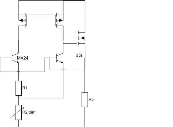
my test results as follows,
-40 (degree) 2.848(V)
-30 2.68
-20 2.531
-10 2.38
0 2.28
10 2.223
20 2.213
30 2.203
40 2.199
50 2.194
60 2.19
70 2.185
80 2.18
90 2.174
100 2.169
110 2.162
120 2.156
Hi Tpeng,
I hope it works. By the way, are you trying to trim only one resistor? What is the topology of your BGR? if you wish, you can upload the figure and we can discuss more about it.
---------- Post added at 15:26 ---------- Previous post was at 15:07 ----------
Hi Samuel,
I see. An output voltage variation of 650 mV between T(-40) and T(40) is not expected.
Is this data result of simulation? In simulation we expected an output voltage variation less than 10 mV in this temperature range.
I could say that an output voltage variation of 50 mV between T(40) and T(120) can happen depending on your conditions (corners, monte carlo simulation, VDD, and so on).
But the behavior of your circuit in low temperatures is not expected.
Are you sure that all transistors are in saturation @-40C?
you need to check the operation (e. g. diode behavior) in this temperature value too.
Does your bandgap implements Banba architecture?
palmeirasHi samuel,
But you simulated it using corner and Monte Carlo models?
How many samples have you measured?
Take a look in this topic:
We have discussed possible reasons for such variations.
In your case, it is clear that the wrong operation only happens in low temperatures. I think that there are transistor in linear region.