Continue to Site

Welcome to EDAboard.com

Welcome to our site! EDAboard.com is an international Electronics Discussion Forum focused on EDA software, circuits, schematics, books, theory, papers, asic, pld, 8051, DSP, Network, RF, Analog Design, PCB, Service Manuals... and a whole lot more! To participate you need to register. Registration is free. Click here to register now.

How to simulate PIN diode in CST MWS with both OFF and ON states

Status
Not open for further replies.
Re: PIN diode in CST MWS

The RLC values for the PIN diode model are going to a) be frequency dependant, and b) depend entirely upon the diode you're using!
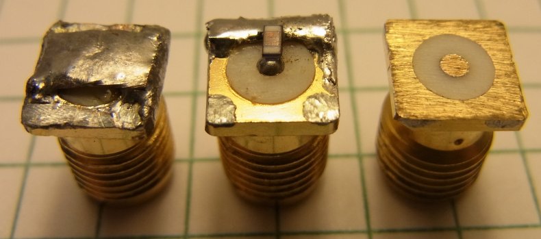
The manufacturer's datasheet would be the first place to look - and if they don't specify what you need, go solder one across an SMA connector and plug it into the network analyser... (with appropriate bias) :)

Hello Sir,


I am using CST Studio Suite 2011 software for designing the Fractral Tree antenna using PIN Diode but I don't know how to use pin diode in CST Studio Suite 2011 software.
So please help me If you have any pdf or step by step instruction or demo project regarding above topic.

Thank you Sir...!!!!
 

Hi all,

I've had a couple of PM's seeking clarification about my flippant instruction:
go solder one across an SMA connector and plug it into the network analyser... (with appropriate bias)

...so I thought I'd elaborate a little :)

As you undoubtedly know, the VNA (network analyser) applies small AC excitations to each of its test ports and measures the energy 'scattered' back (and to its other ports, if applicable.) In the case where the DUT (device under test) is an active component, it's often desired to apply a DC bias in addition to the AC test signal in order to a) bias the component into an active region of interest (i.e. make it work), and b) examine how the scattering parameters change as the bias is changed.

While you *can* add external bias circuitry (as would be required when the device is actually embedded into a circuit), these networks present their own parasitic effects and can obscure detailed, isolated study of the active DUT. An example external bias network is the classic "Bias-T" (https://en.wikipedia.org/wiki/Bias_tee). Every VNA I've ever used offers a nifty alternative though... on the back panel of the R&S ZVB on my desk there are 4 BNC connectors:


If you apply a DC voltage to these connectors, it will be supplied to the corresponding test port of the instrument (which you've coupled directly to your DUT) *without affecting the measurement*! Cool, eh?
The limitations of the bias voltages/currents will be listed in the VNA's manual so check the specifications first, but I've found them to be more than adequate for small-signal LNA to low-power driver amplifier characterisation. I'd never noticed the fuses there before though... undoubtedly a sensible addition by Rohde & Schwarz :)

That's how you apply the PIN diode bias. To test the device itself, solder it across the back of an SMA connector, as illustrated in the following photo:


This photo shows three connectors I used when previously measuring the parasitics of the 43nH 0603 inductor DUT in the centre. (No comments on my soldering please ;)
The other two [identical] connectors are approximations to a "short" and an "open". They are useful to guide you in the adjustment of the instrument's reference plane from that defined during calibration to the plane [position] where your DUT lies on an otherwise identical connector. Sometimes (as my R&S ZVB does) the VNA will incorporate a "fixture compensation" feature which allows you to use these 'short/open terminations' to nudge the internal calibration derived from the precision calibration kit. Alternatively, you can manually adjust the reference plane with each of these terminations connected until the instrument measures sensible impedances (i.e. low for the short and high for the open) for each.

After adjusting the reference plane, you can connect your DUT and apply the desired bias via the rear panel connectors. The instrument will now directly measure the characteristics of your DUT at your desired operating point!
From here you can extract the RLC equivalent parameters for your test frequencies. There are numerous ways to do this, and they range in complexity from simple (i.e. choose a series RLC combination to equal the measured impedance) to complex when a higher order model or broad-band characterisation is required. I recall seeing a number of MATLAB tools in the past, hit Google.

Good luck!
 
Last edited:
  • Like
Reactions: suh

    suh

    Points: 2
    Helpful Answer Positive Rating
Status
Not open for further replies.

Part and Inventory Search

Welcome to EDABoard.com

Sponsor

Back
Top