Continue to Site

Welcome to EDAboard.com

Welcome to our site! EDAboard.com is an international Electronics Discussion Forum focused on EDA software, circuits, schematics, books, theory, papers, asic, pld, 8051, DSP, Network, RF, Analog Design, PCB, Service Manuals... and a whole lot more! To participate you need to register. Registration is free. Click here to register now.

HOW TO SETUP FORWARD & REVERSE BIAS for PIN DIODE in MWO

Status
Not open for further replies.

RFegg

Junior Member level 2
Joined
Oct 28, 2012
Messages
21
Helped
0
Reputation
0
Reaction score
0
Trophy points
1,281
Location
Japan
Activity points
1,459
Hello friends,

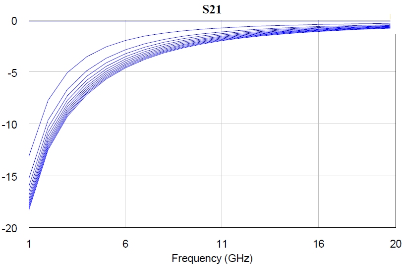
i'm trying to characterize the forward and reverse response of 2 diode models from MWO (PINDD and PIN2) below and above the transit frequency and see that it acts as current controlled resistor at high frequencies.

my question is how to setup the diode as a forward and reverse bias in MWO?
 

It doesn't make sense to reverse-bias the PIN diode because it will act as almost open circuit.PIN diodes are current controlled resistors as you said and they are generally to implement switch circuit or attenuator circuits. A reverse biased PIN diode will behave a voltage controlled capacitor but capacitor values are generally very low ( depending on diode type ) that's why if the frequency is NOT very high, this reverse biased diode capacitance is generally neglected.
 

I think your question is referring how to sweep the DC bias supply of the PIN diode.
From the Sources menu chose DC_V power supply and set VStart, VStop and VStep. Also if you want you can chose for a sweep current supply DC_I.
In the Graph menu set the DC_V to plot all traces.
For example for a series single PIN diode varying the DC bias between -10V and +10V you get a plot similar to the one in the image below.


Re: HOW TO SETUP FORWARD & REVERSE BIAS for PIN DIODE in MWO

It doesn't make sense to reverse-bias the PIN diode because it will act as almost open circuit.PIN diodes are current controlled resistors as you said and they are generally to implement switch circuit or attenuator circuits. A reverse biased PIN diode will behave a voltage controlled capacitor but capacitor values are generally very low ( depending on diode type ) that's why if the frequency is NOT very high, this reverse biased diode capacitance is generally neglected.

Hi Bigboss,

I appreciate your inputs. My application is in switching. I like to have a circuit whose reflection coefficient is 1 or open circuit, with variable angle.
I would have a reversed biased PIN diode and a bank of parallel low value CAPs to vary the phase, as example below;

pindiode.jpg

Diode 1 will be reversed bias permanently, while Diode 2 & 3 can either be open or short.

So my question above how to setup the bias properly in MWO.

Thanks

- - - Updated - - -

I think your question is referring how to sweep the DC bias supply of the PIN diode.
From the Sources menu chose DC_V power supply and set VStart, VStop and VStep. Also if you want you can chose for a sweep current supply DC_I.
In the Graph menu set the DC_V to plot all traces.
For example for a series single PIN diode varying the DC bias between -10V and +10V you get a plot similar to the one in the image below.

Hi Vfone,

I'm getting error on my software using the PIN diode model. Can you send the setup of your circuit in MWO?
 

It doesn't make sense to reverse-bias the PIN diode

**broken link removed**
Abstract - An important circuit design parameter in a high-power p-i-n diode application is the selection of an appropriate applied dc reverse bias voltage. [...]
 

**broken link removed**
Abstract - An important circuit design parameter in a high-power p-i-n diode application is the selection of an appropriate applied dc reverse bias voltage. [...]
Yeah, it's just an caution.PIN diodes are generally used in forward bias.
They say "pay attention the maximum RF voltage swing to make the diode working in safe op area.."
 

PIN diodes are generally used in forward bias.

Sure, for ON state. For OFF state, you usually want to have reverse bias, so that some RF voltage swing does not turn the diode into the "unwanted" forward direction.
 

I have been reading some more on PIN diodes today. I keep going back to my original design which is effectively a shunt attenuator. This is the setup in the attached picture.

shunt limiter.jpg

I was trying to vary the PIN diode resistance with a, appropriate froward current, from Vbias. The only thing that stopped this from working was that the circuit began to oscillate at large RF powers. The DC voltage on the RF line decreased to around -2.5V before this happened. I now know that PIN diodes do self-generate reverse bias when larger RF is put through them. But, I'm unsure of the whole oscillation mechanism. If I can stop this I should be okay.

Is the self-generating reverse bias increasing the PIN diodes resistance, causing the PIN diode to pass less RF and then self-generate less reverse bias, thus going back to a resistive state and so on? This makes sense to me, though I'm not sure how to stop it. I suppose putting more forward bias through it, and increasing the attenuation, would stop it. In practise, as I'll be varying the forward bias to keep my signal at 26dBm, and I may never reach this oscillation point, so I could be safe. It would just be nice to be confident I kow whats going on.
 

Status
Not open for further replies.

Part and Inventory Search

Welcome to EDABoard.com

Sponsor

Back
Top