Continue to Site

Welcome to EDAboard.com

Welcome to our site! EDAboard.com is an international Electronics Discussion Forum focused on EDA software, circuits, schematics, books, theory, papers, asic, pld, 8051, DSP, Network, RF, Analog Design, PCB, Service Manuals... and a whole lot more! To participate you need to register. Registration is free. Click here to register now.

How to reduce DC a bit without resistor or capacitor? Is there a simple solution?

Status
Not open for further replies.
Thank you for your support! I really appreciate that!

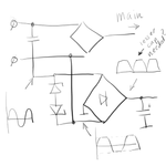
When you said that I should use the the full AC pass, did you mean that I should do something like this?
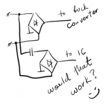
Untitled-1.png

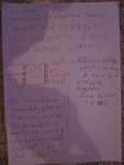
Here is I think what happens in this oscillator:

oscillator2.jpg

When power is applied, capacitors C1 and C2 begin to charge, rising the voltage on the base of the transistor. When it is over a certain level, transistor opens and current begins to flow via transformers winding. Winding on the left produces the spike of voltage that (if the end of the winding connected to capacitor C2), drops the voltage potential on the capacitor C2 to a negative value, thus discharging it quickly. The voltage drops on the base, closing the transistor and cycle starts all over again. Right winding is a voltage rectifier.

Am I correct? :)

Steven
 

Hi Steven
Congratulations ! now you are so close to the path !
ok , now what if you use two back to back zener diode before the auxiliary bridge ? and a capacitor after the bridge ?
by the way the zener can be used after the bridge too .
You are going to the correct path , now ! continue !

Here is I think what happens in this oscillator:

Let me describe it !
In first vision the transistor appears it is biased in class A region ! but it is for transient response ! not anymore !
The resistor which has been tied through the supply voltage is for biasing the transistor at class A region !
when you closing the key ( giving the supply ) there will be a shock or a fast response ! so the current through the base of the BJT will be as it will deliver an instantaneous collector current ! so the tank circuit will take the desired harmonic from that and it will apply it through the base by the magnetizing path .so amplitude is going to be larger ! and it is a sine wave . it will be continued till the transistor is going to be saturated by the signal but the tank circuit which has been created by C1 and the coupled inductor in parallel with that won't allow this to be happened . ( by taking the first harmonic ) ( approx of course )
C2 is just a coupling capacitor to prevent DC bias being grounded via the primary side of transformer . i.e : an inductor will be shorted after five time constant instead of no dv/dt and dphi/dt ( DC signal ) .
So , now the amplitude of feedback path is as large as the transistor can go through the class AB arrangement . so the efficiency will be increased after transient time and the circuit will work as we want ! now the secondary have large value of AC voltage ( high frequency of course ) . but we can decrease it by changing the number of turns . and then a rectifier and limiter and a filter . so we have agood DC voltage as a low power , PSU !
That's all .
Any question about it ?

By the way i think some hours away i can send you those literature about UC3845 !

Best Wishes
Goldsmith
 

Goldsmith,

Here is what I came up with:

Untitled-1.png

I wonder why we would need those zeners? To make sure that the main voltage fluctuations will not affect the voltage on the IC? Or to increase the "duty" of the signal (by clipping tops of the waveforms) so we do can use smaller filter capacitor?

By the way, I forgot to put another zener at the output... Another question. There are voltage regulators that you could buy. What would be an advantage or disadvantage in using them instead of zeners?


As to the oscillator, I think I vaguely understood how it works. But I do not have enough knowledge to figure out what would happen in the LC circuit after the initial surge if current via transistor. Are you saying that it will begin oscillation while transistor still open? Wish I could see a waveform to understand.


I was tied with work this week and could not get to experiment with the circuit... Hopefully tonight...

Steven
 

Hi Steven
First of all , here what i've promised regarding the UC3845 comes :
1.JPG
2.JPG
3.JPG
4.JPG
5.JPG

Take a look through them and ask me if you have any doubt about them .
Here is what I came up with:
Congratulations Steven ! that is what i was meaning ! you could get the idea ! :wink:
I wonder why we would need those zeners? To make sure that the main voltage fluctuations will not affect the voltage on the IC? Or to increase the "duty" of the signal (by clipping tops of the waveforms) so we do can use smaller filter capacitor?
those Zeners have been used to limit the voltage ! don't forget behavior of a capacitor and effect of variations at the input !
By the way, I forgot to put another zener at the output... Another question. There are voltage regulators that you could buy. What would be an advantage or disadvantage in using them instead of zeners?
Some reasons ! first one is high voltage regulators are more expensive than two zener diode and one capacitor !
and zeners are smaller !
And i hope you didn't refer to the voltage regulators like 78xx series because they are dealing with low voltage limitations as vin .
As to the oscillator, I think I vaguely understood how it works. But I do not have enough knowledge to figure out what would happen in the LC circuit after the initial surge if current via transistor. Are you saying that it will begin oscillation while transistor still open? Wish I could see a waveform to understand.
Which section is exactly unclear to you ? are you familiar with oscillators and how they are working ? ( simple oscillators like hartley or perhaps clapp or ... )
i can guide you through the well understanding of the circuit ! :wink:

Good Luck
Goldsmith
 

Goldsmith,

I am still struggling with that boost converter. The IC works OK by itself, but when I apply power to the inductor/MOSFET, it dies...

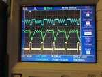
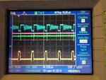
I took the inductor, MOSFET, diode and two electrolytic caps and imitated what happens when I apply 200kHz to MOSFET.

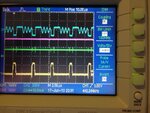
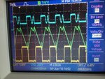
image.jpegimage_1.jpegphoto.JPG

Yellow graph is the voltage applied to the MOSFET's gate. about 10-12V, 200kHz. The total voltage that I applied to this setup was 120V. The output voltage ranged from 150V to 210V, depending on inductor.

Blue - is the voltage across the inductor.

Green (that looks like triangle on the second picture) - current across the inductor.

I tried 3 inductors between 200uH - 300uH, taken from TV power supply. I do not know if they they had right ferrite or any gaps.

What can you tell me by looking at these graphs? How they suppose to look like?
Can you help me to find where I can buy right inductor? If not, how can I make one?


_______

About our last conversation - I understand that back-to-back zeners limit the voltage after the capacitor. But I do not understand the benefit of that. If I am going to use a zener after the bridge, why bother to use these zeners? Also you said "don't forget behavior of a capacitor" - what did you mean by that?

Steven

______________________________________________________________________________________________________________________________________________________________________________

Goldsmith,

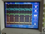
I tried to change the duty of the signal, for an experiment sake, to see if this would affect the waveform.

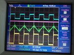
here are 3 pictures (10% duty, 25% and 45%). I was afraid to go over 50%.

Per my understanding, the current across the inductor should have a triangle form. But it is not...

059.JPG060.JPG061.JPG

Is this an inductor issue?

______________________________

I have a question for you - is there any way we could communicate a bit more often? Perhaps by E-mail? or it is your internet connection issue?

Steven


__________________________________________________________________

Goldsmith,

I found a web site that helps calculating the value of the inductor for the boost converter. When I entered my data, it suggested a 2,400uH inductor instead of 200uH that was on the datasheet of FAN7340. It also higher than what is calculated using the formula on the datasheet of FAN7340.

https://www.coilcraft.com/dcdc.cfm

Which value is correct then?

Steven


____________________________________

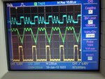
Update: I think I found what the issue was - wrong inductor. I found a new inductor today (got it from Y-board of Panasonic TV). It was 1mH and it worked like a charm! I finally got the current wave form as it should be!!!

Look:

oscilloscope graphs 001.JPG

Green is that desired wave form, blue is the voltage across the inductor. yellow - what goes to the gate and pink is the resulting output voltage. Boy, am I happy!!!!!
That brings me to the question though - how come the final solution was nothing like the formula from FAN7340's datasheet calculated and nothing like the above-mentioned web site calculator produced??? But something in between? By the way, I tried 2.5mH inductor and waveform was not triangle (too much inductance?).

Steven
 
Last edited:

Hi Steven
How are you ?
Sorry for the delayed reply . i can't believe this that my internet again had problem !!!!
Wow ! i can see that you could remove the problem at last , Congratulations for that !
But don't forget an online designer won't let you learn and won't help you to be a designer and it will limit your abilities , of course .
Green is that desired wave form, blue is the voltage across the inductor. yellow - what goes to the gate and pink is the resulting output voltage. Boy, am I happy!!!!!
Ha ha ! i can understand your feeling . now i can remember my first days with SMPS , i had the same feeling when i could build my first one ! ( as i have jumped and some of my families were wondering what happened to me !
( so i highly recommend you to don't jump if your circuit is going to work .) ha ha :-D
That brings me to the question though - how come the final solution was nothing like the formula from FAN7340's datasheet calculated and nothing like the above-mentioned web site calculator produced??? But something in between? By the way, I tried 2.5mH inductor and waveform was not triangle (too much inductance?).
Don't forget that value of inductor is too important in boost converter . if it be too low , then current peak will be increased and the result won't be as it is supposed to be . and when it is too large the spikes will be with large amplitudes and of course waveforms will be out of shape . standard calculation will only suite the aim and guarantee the good waveshape . if you are interested in this case i can tell you how to select proper value of inductor and capacitor for a boost converter .
About my email yes we can . i'm sending you my email address via P.M

Best Wishes and Good Luck
Goldsmith
 

Goldsmith,

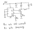
I have a question for you regarding the relationship of the certain items in a buck converter.

I have made a new buck converter based on the HV9861A IC.

The reason I did that is that I am trying to find a solution on how to convert 154V into 125V with the current of 800mA.

The previous buck converter that I built worked very well when the output voltage was 1/3 of the input voltage. I did not like that limitation, so I moved to a different chip. I believe this chip can support my idea.

I was able to make it work with the current of 250mA with the sensing resistor of 0.27ohm, however, when I begin to decrease the sensing resistor Rcs (say, to 0.15ohm) to increase the current via LEDs, the working frequency of HV9861A drops from about 27kHz to 10kHz and it begins to lose stability. If I further decrease the sensing resistor, say to 0.1 ohm, IC practically stops working. Is that suppose to happen? If I use MOSFET with the lower Qg, say, 9, would that help? I tried to change the value of the frequency setting resistor and that did not work. If the value of Rt was too high or too low, generation would stop.

I remember you offered me to use the chip that you like to make a buck converter. If I do that, will this buck converter work with high duty signal? In my case it looks like it should be 0.81!

I feels like I do not understand something. What am I missing?

Steven

Untitled-1.png
 

I have a question for you regarding the relationship of the certain items in a buck converter.

I have made a new buck converter based on the HV9861A IC.

The reason I did that is that I am trying to find a solution on how to convert 154V into 125V with the current of 800mA.

The previous buck converter that I built worked very well when the output voltage was 1/3 of the input voltage. I did not like that limitation, so I moved to a different chip. I believe this chip can support my idea.

Hi Steven
Sorry for the delayed reply .
Yes i believe so . it can be a good option .
I was able to make it work with the current of 250mA with the sensing resistor of 0.27ohm, however, when I begin to decrease the sensing resistor Rcs (say, to 0.15ohm) to increase the current via LEDs, the working frequency of HV9861A drops from about 27kHz to 10kHz and it begins to lose stability. If I further decrease the sensing resistor, say to 0.1 ohm, IC practically stops working. Is that suppose to happen?
Did you use any kind of compensation circuit ( a simple RC circuit ) in your current sensing path ? it can fix the problem .
If I use MOSFET with the lower Qg, say, 9, would that help?
the mosfet can not be cause of these problems however , what kind of mosfet you've used ?
I remember you offered me to use the chip that you like to make a buck converter. If I do that, will this buck converter work with high duty signal? In my case it looks like it should be 0.81!
You can use two UC3845 and two diodes as a simple analog OR network then it can work with higher duty cycle as well . it is kind of trick !

Best Wishes
Goldsmith
 

Status
Not open for further replies.

Part and Inventory Search

Welcome to EDABoard.com

Sponsor

Back
Top