Continue to Site

Welcome to EDAboard.com

Welcome to our site! EDAboard.com is an international Electronics Discussion Forum focused on EDA software, circuits, schematics, books, theory, papers, asic, pld, 8051, DSP, Network, RF, Analog Design, PCB, Service Manuals... and a whole lot more! To participate you need to register. Registration is free. Click here to register now.

How to learn about setting up ports in EM tools

Status
Not open for further replies.

sherry20

Junior Member level 3
Joined
Aug 18, 2009
Messages
29
Helped
0
Reputation
0
Reaction score
0
Trophy points
1,281
Location
N/A
Activity points
1,557
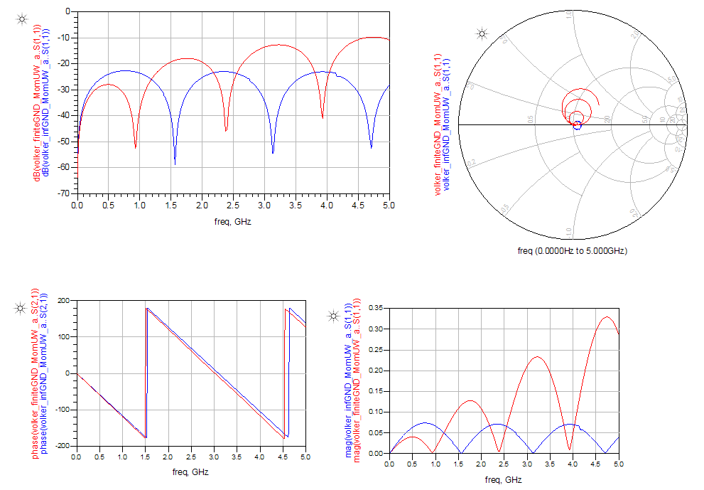
I've been increasingly running into cases where if I set up ports in a simulation in a slightly different way, I get a different answer. Both in Momentum and HFSS/Designer. I know this makes sense because essentially I'm exciting the structure in a different way and there're also port parasitics, but it also make me worry a lot. I realize people with experience would know how to set it up correctly. I'm just wondering, is there any good way to learn these things, for example, through online tutorial, forum, books etc?

Thanks a lot for your comments!

Sherry
 

Yes, ports are among the most important EM topics and it is amazing how few tutorials are published on the underlying concepts. The choice of ground reference for the port is important, and port calibration can also be an issue.

What is your application? For Momentum, I have published a few RFIC/MMIC port appnotes here:
https://muehlhaus.com/support/ads-application-notes/momentum-port-global-ground-or-differential
https://muehlhaus.com/support/ads-application-notes/inductor-em-ports
https://muehlhaus.com/support/ads-application-notes/em_line_ground
https://muehlhaus.com/support/ads-application-notes/edge-area-pins

Thanks, these are awesome materials! I'm focusing on extracting PCB boards using Momentum, and the port setup is a big challenge since I realize I'm getting different results just by setting up the ports differently. Actually I'll just post one of my examples below. Maybe you could shed some light on it :)

- - - Updated - - -

I'm running a simulation for a 50ohm transmission line in Momentum, and have been trying several ways to setup the port. This is an exercise for me to have a better understanding on how to set up simulations in Momentum.

The structure is shown below (see attachment). The signal line thickness is 52.5um, width is 635um, gap width on either side is also 635um and the co-planar grounds are about 6mm wide each. Dielectric thickness is 304um, epsilon_r=3.38. Bottom metal thickness is 35um, but in Momentum, it's set as a sheet. The width is 16mm (finite ground plane). The transmission line is 61mm long.


I've tried several ways of setting up the port. On one end the of line,

a) +P1 -GND (default ideal ground)
b) +P1 - P2,P3 (negative terminal on the two co-planar grounds)
c) +P1 -P4 (negative terminal on the bottom layer only)
d) +P1 -P2,P3,P4 (negative terminals on both side grounds and bottom ground)

In the attachment, I've shown results from b) - d), and result from case a) is very unphysical (+20dB) for some reason.


My questions are:

1) Among the 4 port setups I've tried, what is the correct/mostly used way to set up a port in this type of problem?

2) What could I did wrong to make case a) producing highly unphysical result? I've attached my workspace. I assume it's the finite ground plane, b/c if I replace it with an infinite plane, it works.

3) Why is the additional null show up in one case but not the other two? The fact that it also shows up in the measurement makes me believe it's the correct answer out of the three. My guess is there's some parasitic mode being excited, but I can't provide a good explanation of the phenomena.


Thank you very much for any answers/comments you make.

Regards,

Sherry
 

Attachments

  • MyWorkspace1_50ohm_transmission_line.tar.gz
    12.6 MB · Views: 145

Hi Sherry,

I had a quick look at your model and these issues:

1. The port setup looks wrong/unexpected for CPW. You have added some extra metal near the pins, and then placed the pins inside the metal. This means that you can't use port calibration. Is this to imitate the measured hardware, or any other reason why you created the pins/ports that way? Usually, I would define a proper edge for all signal and return conductors, and place the ports at that edge.

2. Related to 1: it seems that you compare to measurements. How did you feed the hardware in measurement? If we know that, we can use a similar way (more or less) of feeding in Momentum.

3. You have NOT used edge mesh. For accurate results with such lines, edge mesh is highly recommended.

4. You have used mesh reduction. For most accurate results, I would switch it off. It might create an asymmetric mesh for your symmetric layout. Let's play it safe and switch off mesh reduction for this case.

I will look in more detail, and prepare a model for you which I consider accurate. What ADS version do you use?

Regards
Volker

- - - Updated - - -

a) +P1 -GND (default ideal ground)

2) What could I did wrong to make case a) producing highly unphysical result?

This case can't work because there is no physical return path. Your CPW ground isn't connected at all, and there is not infinite ground plane in the substrate definition either. With an infinite ground, Momentum would automatically place the port reference at the nearest infinite ground location. Without such infinite ground, you must manually provide an explicit ground reference that is physically close to the signal pin. Otherwise, results will make no sense.
 
  • Like
Reactions: sherry20

    sherry20

    Points: 2
    Helpful Answer Positive Rating
    V

    Points: 2
    Helpful Answer Positive Rating
Hi Sherry,

I had a quick look at your model and these issues:

1. The port setup looks wrong/unexpected for CPW. You have added some extra metal near the pins, and then placed the pins inside the metal. This means that you can't use port calibration. Is this to imitate the measured hardware, or any other reason why you created the pins/ports that way? Usually, I would define a proper edge for all signal and return conductors, and place the ports at that edge.

2. Related to 1: it seems that you compare to measurements. How did you feed the hardware in measurement? If we know that, we can use a similar way (more or less) of feeding in Momentum.

3. You have NOT used edge mesh. For accurate results with such lines, edge mesh is highly recommended.

4. You have used mesh reduction. For most accurate results, I would switch it off. It might create an asymmetric mesh for your symmetric layout. Let's play it safe and switch off mesh reduction for this case.

I will look in more detail, and prepare a model for you which I consider accurate. What ADS version do you use?

Regards
Volker

- - - Updated - - -


This case can't work because there is no physical return path. Your CPW ground isn't connected at all, and there is not infinite ground plane in the substrate definition either. With an infinite ground, Momentum would automatically place the port reference at the nearest infinite ground location. Without such infinite ground, you must manually provide an explicit ground reference that is physically close to the signal pin. Otherwise, results will make no sense.

Hi, Volker,

Thanks a lot for your help. Here's some more info regarding the issues you mentioned:

1. The extra piece of metals were in the layout when I got the file. I think it corresponds to the actual shape of the fabricated board. There are two pieces of ground/copper stick out in the lateral direction so that the SMA connectors won't short all metal layers in the board. I think I moved the port inside because in some of the cases where I place a port with + terminal as the signal line and - terminal on bottom layer, the bottom layer right below the signal line does not have the extension. In order to maintain a straight port line, I decided to move everything inside, so they are at the same lateral position from the top view. I know this sounds a bit weird, maybe causing trouble too, because in some case, I just deleted the two small pieces to make it easier.

2. The hardware is excited using SMA, which has 1 center pin and 4 ground pin. The two ground pins on the bottom of the board is not modeled in ADS because 1) I deleted the actual bottom layer to simplify a 4-layer board to 2-layer and 2) To draw a port line b/w the 2 bottom ground pads for SMA to the signal line, the port lines will be slanted and I think undesirable.

3,4 Thanks for your insightful suggestion, I left everything as default because I didn't know what should I touch.

5) Regarding the default ground, I understand it's causing problem and I can do an easy fix in this case, but I have some question for another design I've encountered. So I had a 4 layer board, and none of the layers is a solid ground plane, so I realized I have to use the theoretical infinity ground. Then I worry about the accuracy of my result. In this case, is there any other way I can setup the port to avoid using the theoretical ground?

Thank you very much!
 

Hi Sherry,

1. The extra piece of metals were in the layout when I got the file. I think it corresponds to the actual shape of the fabricated board. There are two pieces of ground/copper stick out in the lateral direction so that the SMA connectors won't short all metal layers in the board.

Ok, makes sense.

So now the question is: do we want to model in Momentum the same excitation that you have measured, or the line only (excluding feed effects)?

I assume that you want to model the measured case, and then the lower ground plane must not be connected with a (-) pin because there is no such connection in your measurement.

I have placed my (-) (+) (-) ports at the outer edge, because this seems to be closer to your measured scenario.


With this, I simulated two cases: with finite (drawn) ground below, and with infinite ground. (Pictures below can't be compared directly because frequency and scale is different, but you see what I modelled...)


I think the best way to understand the results is the Smith chart here. You can see that the infinite ground results show decent match, whereas the finite ground moves towards the inductive region.


The difference can be understood as extra series inductance for the finite ground case, or less shunt capacitance for the finite ground case, or a combination of that. If we think about the extra notches at the ground pin location, this makes physical sense: more series L and less shunt C if we remove the ground below these notches. To me, this effect makes sense and looks real.

In the attached workspace, I have included a schematic to play around with these parasitic L and C.

You can see that the S11 zeros (frequency) now match up decently with your measured values, but the absolute value is off. If you play around with the parasitic L and C, you will notice that very minor changes also increase/decrease the S11 magnitude. I suspect that we have some parasitic effect there in the SMA connection/soldering in measurement that we haven't exactly modelled in Momentum. Minor parasitics matter here, as we look at rather good matching levels.

3,4 Thanks for your insightful suggestion, I left everything as default because I didn't know what should I touch.

For best accuracy, I recommend these two changes to the mesh options:


5) Regarding the default ground, I understand it's causing problem and I can do an easy fix in this case, but I have some question for another design I've encountered. So I had a 4 layer board, and none of the layers is a solid ground plane, so I realized I have to use the theoretical infinity ground. Then I worry about the accuracy of my result. In this case, is there any other way I can setup the port to avoid using the theoretical ground?

The individual S-parameters (port referenced to ground at infinity) will be invalid then, but you will get useful results as soon as you assign another physical pin as the explicit ground reference. This can be done on the port settings, and you had already use that option. If you had already done/tried that in your "strange results" case, I would suspect that you mixed up pin numbers and assigned wrong reference pins (physically far away from the signal pin).

Archived ADS2014 workspace is attached.
 

    V

    Points: 2
    Helpful Answer Positive Rating
Hi Sherry,
The individual S-parameters (port referenced to ground at infinity) will be invalid then, but you will get useful results as soon as you assign another physical pin as the explicit ground reference. This can be done on the port settings, and you had already use that option. If you had already done/tried that in your "strange results" case, I would suspect that you mixed up pin numbers and assigned wrong reference pins (physically far away from the signal pin).

Archived ADS2014 workspace is attached.

Hi Volker,

Thank you so much for all these explanations. I'll spend more time looking at your comments and try a few things as you suggested. Just wondering, did you attached the modified workspace? I wanna see how you played with the schematic, but I don't see the attachment from my end.

Thanks again,

Sherry
 

Just wondering, did you attached the modified workspace? I wanna see how you played with the schematic, but I don't see the attachment from my end.

Sorry, it wasn't attached. Here it is.
 

Attachments

  • CPW_Line_wrk.zip
    1.6 MB · Views: 85

    V

    Points: 2
    Helpful Answer Positive Rating
Sorry, it wasn't attached. Here it is.

Hi Volker,

Thanks, I looked at your model for discontinuity and it's really inspiring! Now I can see how extra L or C makes a difference here. I just have a few more questions.

1) When I place the ports slightly inside, not at the edge of the small rectangles, the amplitude of S11 is lower and matches better with measurement. Do you think this make sense? I realize the SMA is in contact with the board for about 5mm long from the edge toward the middle, so I suppose it's hard to say whether the excitation is at the edge or the tip of SMA connector.

2) I turned on the edge mesh and turned off the mesh reduction, and it makes the result match better with the measurement. I see there's also a transmission line mesh, and it'll make denser mesh on the signal line. When should I use that?

Thanks,

Sherry
 

Hi Sherry!

1) When I place the ports slightly inside, not at the edge of the small rectangles, the amplitude of S11 is lower and matches better with measurement. Do you think this make sense? I realize the SMA is in contact with the board for about 5mm long from the edge toward the middle, so I suppose it's hard to say whether the excitation is at the edge or the tip of SMA connector.

Makes sense to me ... the connection through the extra metal strip for the side grounds is inductive, and if we add solid solder connection, we reduce inductance, which helps to improve the matching.

2) I turned on the edge mesh and turned off the mesh reduction, and it makes the result match better with the measurement. I see there's also a transmission line mesh, and it'll make denser mesh on the signal line. When should I use that?

For coupled lines (signal and ground in the CPW) most the capacitive charge goes to the edges (gap). We want to have fine mesh there, so that the solver can place the charge at the gap. That's exactly what edge mesh gives us: fine mesh along the conductor edges.

I have not much experience with transmission line mesh in Momentum, but from my experience with other tools and from looking at the current densities for lines, I would think that edge mesh is the better choice in most cases (where line width >> skin depth).
 

    V

    Points: 2
    Helpful Answer Positive Rating
Hi Sherry!


Makes sense to me ... the connection through the extra metal strip for the side grounds is inductive, and if we add solid solder connection, we reduce inductance, which helps to improve the matching.


For coupled lines (signal and ground in the CPW) most the capacitive charge goes to the edges (gap). We want to have fine mesh there, so that the solver can place the charge at the gap. That's exactly what edge mesh gives us: fine mesh along the conductor edges.

I have not much experience with transmission line mesh in Momentum, but from my experience with other tools and from looking at the current densities for lines, I would think that edge mesh is the better choice in most cases (where line width >> skin depth).

I see. I get pretty good match b/w simulation and measurement for S11 now. I still have some issue with S21, the simulated value is always higher than the measured value. Since S11^2+S21^2 != 1 in reality because of losses, I think the simulation didn't catch all the losses that present in the measurement, although it catches some of the losses. I'm just wondering if there is any setting i should play with to include more loss effect in the result. Now I have the tangent loss of the dielectric, and copper conductivity is 5.8e7, I'm using Momentum microwave, so it should already count the radiation loss. Is there anything else I should be aware of to have a better matched S21?

Thanks a lot!

Sherry
 

some issue with S21, the simulated value is always higher than the measured value.

Not sure if "higher" refers to transmission, or insertion loss? Do you mean the measurement has more loss?

- - - Updated - - -

When I looked for the roughness value of the RO4003 copper foil, to include it in simulation, I noticed that Rogers only offers 18µm, 35µm and 70µm coper foil thickness. What is the 52.5um thickness that you mentioned - any extra metals like nickel/gold on top of the copper?

Um...I'm not sure if I understood it correctly, I thought RO4003 is the dielectric, and the copper is on top of the Rogers material, not inside. The copper trace is 1.5oz, which translates to 52.5um. I don't think there's other metal on top of it.

For the S21, I meant the measurement has more loss, and thus a lower numerical value for S21.
 

Um...I'm not sure if I understood it correctly, I thought RO4003 is the dielectric, and the copper is on top of the Rogers material, not inside.

Sure, it is on top. I'm just surprised by the 1.5oz because in the Rogers documentation there is no such metalization option. They have listed 1/2oz, 1oz and 2oz only.


I had simulated with 3.2µm RMS roughness for the bottom side of the conductor, which caused an increase in insertion loss of ~ 0.05dB at 5GHz for your line.

The copper trace is 1.5oz, which translates to 52.5um. I don't think there's other metal on top of it.

Ok, fine. I was thinking that you might have Nickel/Gold passivation on top, which is known to increase the losses.
 

    V

    Points: 2
    Helpful Answer Positive Rating
Sure, it is on top. I'm just surprised by the 1.5oz because in the Rogers documentation there is no such metalization option. They have listed 1/2oz, 1oz and 2oz only.


I had simulated with 3.2µm RMS roughness for the bottom side of the conductor, which caused an increase in insertion loss of ~ 0.05dB at 5GHz for your line.


Ok, fine. I was thinking that you might have Nickel/Gold passivation on top, which is known to increase the losses.

Oh...I always ignored the copper surface roughness, I looked at the table you attached, and don't quite understand the first column, how do I know which foil type my board is using? Should the PCB vendor have the info or is there something general I can assume?
 

Oh...I always ignored the copper surface roughness

Same for me :wink:

I only included it here, because the software can do it, and we are looking for sources of extra loss.

I looked at the table you attached, and don't quite understand the first column, how do I know which foil type my board is using? Should the PCB vendor have the info or is there something general I can assume?

There are two main kinds of copper metalization that Rogers offers: smooth (rolled) copper and electrodeposited (rough) coppen. Smooth has lower losses, rough is more stable (peel-off) over thermal cycles. You can really buy both, so it is difficult to guess what you have. Your PCB vendor will know what he ordered.
 

Same for me :wink:

I only included it here, because the software can do it, and we are looking for sources of extra loss.


There are two main kinds of copper metalization that Rogers offers: smooth (rolled) copper and electrodeposited (rough) coppen. Smooth has lower losses, rough is more stable (peel-off) over thermal cycles. You can really buy both, so it is difficult to guess what you have. Your PCB vendor will know what he ordered.

Hi Volker, sorry to bug you again, I ran into a new issue with the same case. Last time, I did the simulation based on a 2 metal layer board. The original board has 4 metal layers, of which the bottom 3 layers are just solid ground planes connected through vias. So I deleted the bottom two to simplify the problem. Now I try to include all four layers in the simulation, and the result start to show simulation artifacts around 3.5-5GHz, as in the attached plot.

I'm wondering if I'm doing something wrong again, and how to tune the simulation so that it'll produce a correct simulation result based on the original 4 layer PCB.
Thanks a lot!

Sherry
 

Attachments

  • MyWorkspace1_wrk_0922_4metal.tar.gz
    17.9 MB · Views: 531

Why? Do you expect any effect from multiple ground layers in parallel?

Oh, because I want to make sure the simulation is still accurate if I don't know how to simplify the problem and just give the whole thing to the simulator. Also, most of the real PCB I work with are 4 layers without possible simplification, and I see similar resonance at higher frequency from time to time. I always wonder if they're real...

Another thing is, I was gonna show how the simplification of geometry doesn't change the result, and now I can't explain why the original structure doesn't work :p
 

Hi Volker, do you have any suggestion on what I can try? I still haven't figured out this problem...
 

Status
Not open for further replies.

Part and Inventory Search

Welcome to EDABoard.com

Sponsor

Back
Top