geozog86
Member level 3
How to change VDS/VDSSAT
Hello!
I have a funny very basic but very confusing situation.

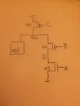
I have the circuit you see in the graph: a tail transistor M1 has a set gate voltage C, so it's acting as a current source.
The branch I care about has a current source (transistor M3, with gate voltage A set, so set vgs), so I know the current I am taking in this branch from the tail transistor.
Then I have the transistor M2, with externally set gate voltage B.
My understanding is that by having VB set, and current through M2 set, I'm setting TAIL voltage (so Vgs of M2 is the appropriate value).
Here's the fun: How do I control VD in order to change VDS of M2?
There are a few corners in which M2 enters linear region. In those corners resizing the transistor (I made L longer for example) changes VDS, but at the same time so does VDSSAT since VGS is changing, and I remain in linear. Plus that change only makes VTAIL change-VD stays pretty constant.
So (the general question is) how do I change VDS without changing VDSSAT? Or How do I control V at node D. Or how do I bring a transistor in saturation from linear with minimal changes?
((FYI there may be many ways, but I can't change for example biasing in node B....Unfortunately!))
Cheers for any kind of idea (circuit specific or general lesson on biasing, both will be appreciated)
Hello!
I have a funny very basic but very confusing situation.

I have the circuit you see in the graph: a tail transistor M1 has a set gate voltage C, so it's acting as a current source.
The branch I care about has a current source (transistor M3, with gate voltage A set, so set vgs), so I know the current I am taking in this branch from the tail transistor.
Then I have the transistor M2, with externally set gate voltage B.
My understanding is that by having VB set, and current through M2 set, I'm setting TAIL voltage (so Vgs of M2 is the appropriate value).
Here's the fun: How do I control VD in order to change VDS of M2?
There are a few corners in which M2 enters linear region. In those corners resizing the transistor (I made L longer for example) changes VDS, but at the same time so does VDSSAT since VGS is changing, and I remain in linear. Plus that change only makes VTAIL change-VD stays pretty constant.
So (the general question is) how do I change VDS without changing VDSSAT? Or How do I control V at node D. Or how do I bring a transistor in saturation from linear with minimal changes?
((FYI there may be many ways, but I can't change for example biasing in node B....Unfortunately!))
Cheers for any kind of idea (circuit specific or general lesson on biasing, both will be appreciated)
Last edited: