Continue to Site

Welcome to EDAboard.com

Welcome to our site! EDAboard.com is an international Electronics Discussion Forum focused on EDA software, circuits, schematics, books, theory, papers, asic, pld, 8051, DSP, Network, RF, Analog Design, PCB, Service Manuals... and a whole lot more! To participate you need to register. Registration is free. Click here to register now.

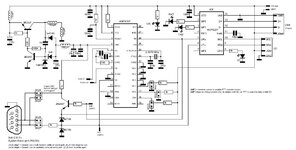
How does this UART to RS-232 converter work?

Status
Not open for further replies.

neazoi

Advanced Member level 6
Joined
Jan 5, 2008
Messages
4,148
Helped
13
Reputation
26
Reaction score
15
Trophy points
1,318
Location
Greece
Activity points
37,119
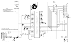
How does this UART to RS-232 converter work?


I see a negative charge pump, which is driven by an oscillator (200khz square wave, internal to the chip).
Then the PNP switches between a negative voltage of the pump and the positive (depended on the data on it's base pin), for the differential requirements of the RS-232 (compatible). But how does it do this switching, I am confused.
 

Attachments

  • schematic_simple.gif
    schematic_simple.gif
    36.2 KB · Views: 266
Last edited:

For Tx, my guess is that the TTL level signal from pin 18 of the MCU will turn on or off T2 which will toggle the RS232 voltage between the +ve and -ve voltage levels for that standard.
The emitter of T2 is held to +5V which means that it will drag the collector to +5V when it conducts and lets the collector float to the -ve voltage when it shuts off.
The base voltage will be driven by the MCU and so will be between 0 and +5V and that is enough difference to the emitter voltage to do the switching.
For Rx, they just limit the voltage swing using D2 to TTL acceptable levels being fed into pin 15 of the MCU.
My opinion: this will be OK for personal/non-commercial use but I would not like to see it in a commercial device - there are SO MANY TTL/RS232 converters out there that are designed to exactly this job so why not use one of those. It also leaves the MCU free to do other useful work (other than being a glorified oscillator/voltage pump).
Susan
 

    neazoi

    Points: 2
    Helpful Answer Positive Rating
The emitter of T2 is held to +5V which means that it will drag the collector to +5V when it conducts and lets the collector float to the -ve voltage when it shuts off.
But how can the collector be at +5v when the transistor is switched on? Won't it cancel out with the negative voltage provided by the charge pump?

As far as the receiver concerns, I think D2 converts -5v to 0v and D3 is the one that limits the positive voltage. So for example is the positive voltage that comes into the port is +12v, D3 will conduct and send the exessive voltage to +5v (????). Can it be true?
 

But how does it do this switching, I am confused

It doesn't !

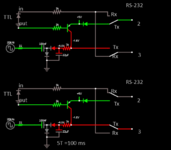
1632273284122.png

Not only is it R2L but PNP upside down. bad form.

Who says this Rx/Tx even works?
D2 clamps any negative voltage on pin 2. That seems to be a bipolar voltage violation for the Tx option.

I see Rx from pin 2 but do not see any Rx from pin 3.
Conclusion: Not recommended.

This is how I would make it work.


Rev A
1632273725746.png


The DPDT are just 2 jumpers options

The analog Rx threshold for RS-232 is 2 diode drops or 1.3V but is bipolar for margin. Schottky diode for Rx, pump
 

Attachments

  • 1632273155381.png
    1632273155381.png
    27.6 KB · Views: 174
Last edited:

    neazoi

    Points: 2
    Helpful Answer Positive Rating
It doesn't !

View attachment 171973
Not only is it R2L but PNP upside down. bad form.

Who says this Rx/Tx even works?
D2 clamps any negative voltage on pin 2. That seems to be a bipolar voltage violation for the Tx option.

I see Rx from pin 2 but do not see any Rx from pin 3.
Conclusion: Not recommended.

This is how I would make it work.


Rev A
View attachment 171974

The DPDT are just 2 jumpers options

The analog Rx threshold for RS-232 is 2 diode drops or 1.3V but is bipolar for margin. Schottky diode for Rx, pump
Thanks for your reply, but it actually works. RS-232 communications with this scheme at 1200 baud, have been tested many times, with communication of the device with PC, serial dial-up modems, and device-to-device. So it must work somehow.

I am not sure I understand your description of why it doesn't work?
 

Hi,

it may work, but I guess not according specifications.

The circuit around C1 is a voltage inverter.
R3 pulls the signal to negative voltage (which is HIGH for RS232)
T2 pulls the signal to positive voltage (which is LOW for RS232)

I expect close to +5V, but only about -4V due to voltage drops.

D2 and D3 are used as voltage limiter for the RxD input.
I don´t know whether R1 is according specifications.

I don´t have the RS232 levels in mind. Often one sees threshold levels +3V and -3V. But I think this are the levels for inputs.
Outputs should have higher levels to get a noise margin and to care for voltage drop and ground bounce.

As said I don´t know the specifications, but I find the -4V critical.

Klaus
 

    neazoi

    Points: 2
    Helpful Answer Positive Rating
Hi,

it may work, but I guess not according specifications.

The circuit around C1 is a voltage inverter.
R3 pulls the signal to negative voltage (which is HIGH for RS232)
T2 pulls the signal to positive voltage (which is LOW for RS232)

I expect close to +5V, but only about -4V due to voltage drops.

D2 and D3 are used as voltage limiter for the RxD input.
I don´t know whether R1 is according specifications.

I don´t have the RS232 levels in mind. Often one sees threshold levels +3V and -3V. But I think this are the levels for inputs.
Outputs
should have higher levels to get a noise margin and to care for voltage drop and ground bounce.

As said I don´t know the specifications, but I find the -4V critical.

Klaus
RS-232 levels are:
-3 to -25v for logic 1
+3 to +25v for logic 0

This is why I said, it is compatible, but it is a low voltage RS-232. However I have found no problems communicating with devices near-by.

But what I do not understand is how the transistor switching works. When T2 is energised, at it's collector presents +5v. But how does this +5v interact with the -5v of the charge pump circuit? Shouldn't they be eliminate and equal to 0v?
 

Hi,

But what I do not understand is how the transistor switching works. When T2 is energised, at it's collector presents +5v. But how does this +5v interact with the -5v of the charge pump circuit? Shouldn't they be eliminate and equal to 0v?
T2_emitter is +5V
T2_collector is TxD
T2_base is via resistor to microcontroller_TxD

So when microcontroller is HIGH:
then T2 is high impedance and the TxD voltage is determined by the negative voltage supply through R3 --> -4V

When microcontroller is LOW:
then T2 is low impedance (much lower than R3) thus the voltage is almost --> +5V

****

signal voltage:
Imagine there are two identical devices communcating with each other.
One (sender) is driving the signal (wire) via 1k to -4V.
the other end (receiver) is pulling the signal via R1 and D2 to -0.3V (estimated)
then the wire voltage will be about -2.15V.
Clearly in the "unallowed area" between -3V and +3V.

Thus my worries about the -4V, R1, R3 and D2...

It´s not the -4V at the negative supply that counts. It´s the-2.15V signal voltage at the wire.

Klaus
 

    neazoi

    Points: 2
    Helpful Answer Positive Rating
If I understand the initial post right, you have problems to understand (already verified) circuit operation. Surprizing to hear people explaining that it can't work at all.

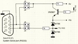
I confess to have used similar single transistor PNP RS-232 TxD drivers in industrial products, they are working since more than 30 years. Besides missing ESD protection of the TxD line in the original design shown below, the circuit is quite robust. Notice that it was released before EMV CE regulations. A possible disadvantage is 1k TxD output impedance. The peer receiver might catch edges of its own Tx signal when connected through a long cable > 10 m.

1632298010245.png
 

Hi,


T2_emitter is +5V
T2_collector is TxD
T2_base is via resistor to microcontroller_TxD

So when microcontroller is HIGH:
then T2 is high impedance and the TxD voltage is determined by the negative voltage supply through R3 --> -4V

When microcontroller is LOW:
then T2 is low impedance (much lower than R3) thus the voltage is almost --> +5V

****

signal voltage:
Imagine there are two identical devices communcating with each other.
One (sender) is driving the signal (wire) via 1k to -4V.
the other end (receiver) is pulling the signal via R1 and D2 to -0.3V (estimated)
then the wire voltage will be about -2.15V.
Clearly in the "unallowed area" between -3V and +3V.

Thus my worries about the -4V, R1, R3 and D2...

It´s not the -4V at the negative supply that counts. It´s the-2.15V signal voltage at the wire.

Klaus
Thank you it is clear not to me of how the circuit works.
It might be that the estimation of -4v is too aggressive. There are low drop diodes used and the current drawn is very little. At the input of the charge pump there is a 200KHz full swing 0-5v oscillator, so maybe the voltage drop is not that much. I will measure it, I am curious.

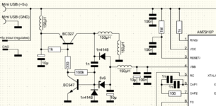
I would like to use the RS-232 circuit with another inverter (non-charge pump) that already produces -5v and avoids this drop you mention. Here it is. Do you think it will work? I do not see why not, but you may have another idea.
 

Attachments

  • rs232.PNG
    rs232.PNG
    26.3 KB · Views: 174
  • inverter.PNG
    inverter.PNG
    49.8 KB · Views: 153

Hi
It might be that the estimation of -4v is too aggressive. There are low drop diodes used and the current drawn is very little.
Yes, it´s just an estimation.
If you have the circuit by hand then you may do some measurements. But mind: with connected receiver.

And the receiver is the point. Or better say the current the receiver draws.
If it´s an identical circuit then it may be a couple of milliamperes (I expect 2.1mA) ... I don´t call it "very little".

Ohms law ... voltage drop .. resulting in 2.1V voltage at the wire...

Klaus
 

It works but poorly.

TTL is inverse (negative) logic to RS-232, and both have the same analog threshold.

Rx clamps negative voltage but does NOT invert, so it must be done in software.

The gnd symbol is non-IPC standard.
It is upside down to IPC stds.
Thanks for your reply, but it actually works. RS-232 communications with this scheme at 1200 baud, have been tested many times, with communication of the device with PC, serial dial-up modems, and device-to-device. So it must work somehow.

I am not sure I understand your description of why it doesn't work?
Sorry but the reversed upside down schematic against IPC standards threw a curve ball.

The PNP is just an inverter with 1k to -V and collector pullup to V+

The Rx also needs an inverter as RS232 to TTL is inverted logic, so it had to be done in S/W

1632315039976.png


RS-232 allows +/- 3V for short connections, yet the Analog threshold is the same as TLL 1.3V but TTL data is inverted logic .
--- Updated ---

Thank you it is clear not to me of how the circuit works.
It might be that the estimation of -4v is too aggressive. There are low drop diodes used and the current drawn is very little. At the input of the charge pump there is a 200KHz full swing 0-5v oscillator, so maybe the voltage drop is not that much. I will measure it, I am curious.

I would like to use the RS-232 circuit with another inverter (non-charge pump) that already produces -5v and avoids this drop you mention. Here it is. Do you think it will work? I do not see why not, but you may have another idea.
RC pump is adequate
 
Last edited:

It works but poorly.

TTL is inverse (negative) logic to RS-232, and both have the same analog threshold.

Rx clamps negative voltage but does NOT invert, so it must be done in software.

The gnd symbol is non-IPC standard.
It is upside down to IPC stds.

Sorry but the reversed upside down schematic against IPC standards threw a curve ball.

The PNP is just an inverter with 1k to -V and collector pullup to V+

The Rx also needs an inverter as RS232 to TTL is inverted logic, so it had to be done in S/W

View attachment 171988


RS-232 allows +/- 3V for short connections, yet the Analog threshold is the same as TLL 1.3V but TTL data is inverted logic .
--- Updated ---


RC pump is adequate

I am confused a bit on your post. What do you mean by inverted, negative voltage, inverted logic, what?

I present a list below on the different standards, including bell103 and bell202 (am7910 modem IC).
Are these correct?

UART:
Idle = 5v
Logic low = 5v
Logic high = 0v

RS-232:
Idle = -3 to -15v
Logic low (space) = +3 to +15v
Logic high (mark) = -3 to -15v

AM7910:
Idle = logic high (mark)
Logic low (space) = 0v
Logic high (mark) = +5v
 
Last edited:

Yes the UART is negative logic . "0"=5V, "1" =0V

But RS-232 inverts negative logic to become positive logic. Rx > 1.3V= "1", < 1.3V="0" They use large bipolar swings to add margin for ringing and crosstalk,

I suggest you read/use the MAX232 specs.

1632316098916.png
 

Yes the UART is negative logic . "0"=5V, "1" =0V

But RS-232 inverts negative logic to become positive logic. Rx > 1.3V= "1", < 1.3V="0" They use large bipolar swings to add margin for ringing and crosstalk,

I suggest you read/use the MAX232 specs.

View attachment 171989
So my list below is correct?
I am not sure about the AM7910, it should be uart compatible, so I may have the voltage levels wrong?

UART:
Idle = 5v
Logic low = 5v
Logic high = 0v

RS-232:
Idle = -3 to -15v
Logic low (space) = +3 to +15v
Logic high (mark) = -3 to -15v

AM7910:
Idle = logic high (mark)
Logic low (space) = 0v
Logic high (mark) = +5v
 

Edit: Apologies (brainfart)+ Yes all your levels are correct .

RS-232 is negative logic
UART is positive logic.

AM7910 has RS-232 negative logic interface but TTL voltages and same thresholds by design.

TTL RD/TD is positive logic.

1632321897920.png

I need coffee.
 

The AVR circuit in post #1 is apparently inverting RxD in software, it uses pin 18 instead of dedicated UART pin 14. At least AM7910 would need an external inversion, the modem chip has no option to provide it.
--- Updated ---

I don't agree with the previous post. AM7910 uses TTL UART level, 1=mark (idle state).
--- Updated ---

AM7910 has RS-232 negative logic interface
May be I misunderstand this sentence. In any case, the chip needs inverting RS-232 interface, RxD inversion is missing in the above AM7910 schematic.
 
Last edited:

Murphy's Law If anything can be inverted, it will be.

FvM is correct as was my paste from AM7910
1632323689460.png
and comment about S/W inverting Rx in AVR cct..

but
UART: shud be
Idle = 5v=mark = "1" positive logic or TTL levels as in the Am7910
Logic low = 0 V not 5V
1632324764078.png


sorry for added confusion.

1632324023679.png

1632324035313.png

 
Last edited:

It is a bit confusing. So the modem IC needs inversion of the TTL levels in both the inputs and outputs?

Here is the current unfinished schematic I have come up with. Maybe this gives you a better idea for suggestions in the specific schematic, so as to avoid mistakes?
 

Attachments

  • modem3.JPG
    modem3.JPG
    65.9 KB · Views: 130

Hi,

it's not a question of "modern" nor "IC".
It's a question of standards.

Standard UARTs are idle HIGH (5V)
RS232 is also idle HIGH, but this is negative voltage (-5V).

Klaus
 

Status
Not open for further replies.

Part and Inventory Search

Welcome to EDABoard.com

Sponsor

Back
Top