circuitking
Full Member level 5
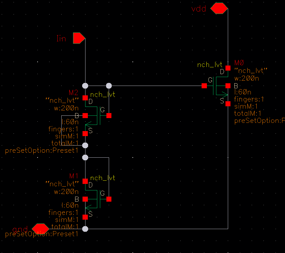
Hi, I wanted to figure out what happens connecting bulk to source or ground terminal in the below circuit. In DRC, it doesn't give any error for the same layout, whether I connect the bulk to source or ground in schematic.
Are there any rules when to connect bulk to source or ground? I usually connect NMOS to ground in all my design, but I want to correct myself if I am doing wrong.
I know connecting bulk to source (if source is higher potential than ground), the threshold voltage decreases. But doing so, do I have to have another P+ contact in the layout for that particular NMOS? In that case, with respect to layout area, it is advantageous to connect all NMOS bulk to ground itself, so that not many P+ contacts are needed.