Welcome to our site! EDAboard.com is an international Electronics Discussion Forum focused on EDA software, circuits, schematics, books, theory, papers, asic, pld, 8051, DSP, Network, RF, Analog Design, PCB, Service Manuals... and a whole lot more! To participate you need to register. Registration is free. Click here to register now.
This amplifier will be used for power amplifier thah it is work at 3-30Mhz frequency range. And input power will be max 0.5W and output power will be 4-5W. Also Av=50 and BD135 will be used. Circuit diagram is attached. How can i design this amplifier ?
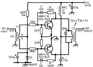
BD135 is an audio dedicated transistor. It can give about 5W RF output power at 3MHz, but at 30MHz cannot get more than 100mW output power.
You have to chose a different transistor, and recommended topology for a broadband PA in HF is push-pull using balun transformers.
This amplifier will be used for power amplifier thah it is work at 3-30Mhz frequency range. And input power will be max 0.5W and output power will be 4-5W. Also Av=50 and BD135 will be used. Circuit diagram is attached. How can i design this amplifier ?
Well first you want to make sure your gain is 40, now if analyze this first using DC voltage, you get the gain to be -(R1/R2) = Av. This is a standard topology
you can derive it if you want but im sure this is correct. Choose the resistors to give you this gain so that also the transistor is in saturation, i.e Vbase > Vcollector.
With that now you can focus on setting the bandwidth.
The first Capacitor is going to set your high frequency. Fh = 1/(2*pi*Rin*C1)
The Second Capacitor is going to set your low frequency. Fl = 1/(2*pi*Rout*C2)
Sometimes i would get these mixed up backwards. This also is all from memory so if i made a mistake anyone please tell me.
Also i forgot to mention, Rin = R (source/sig) + (R3//R4)
Rout = R1//RL
there are also other resistances of the BJT that are present but they are small factors. If you are going for high precision i can help
get a more accurate answer. (for example re value)
I did forget to find the AC gain you are correct, and yes gm = Ic/Vt, given that Vt ~ 26mV, gm ~ 38Ic which is close enough to 40Ic
Thank you for clearing that up
This site uses cookies to help personalise content, tailor your experience and to keep you logged in if you register.
By continuing to use this site, you are consenting to our use of cookies.