Continue to Site

Welcome to EDAboard.com

Welcome to our site! EDAboard.com is an international Electronics Discussion Forum focused on EDA software, circuits, schematics, books, theory, papers, asic, pld, 8051, DSP, Network, RF, Analog Design, PCB, Service Manuals... and a whole lot more! To participate you need to register. Registration is free. Click here to register now.

[SOLVED] HMC 772 Power Amplifier problem

Status
Not open for further replies.

guytoub

Full Member level 2
Joined
Dec 23, 2004
Messages
123
Helped
4
Reputation
8
Reaction score
5
Trophy points
1,298
Activity points
924
Helle Guys;

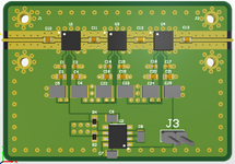
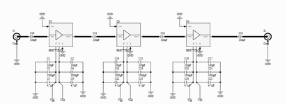
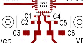
I cascaded three HMC772 amplifiers with a gain of 15dB and a noise figure of 1.8dB. When I measure the final noise figure I have 7.5dB.
The final gain is indeed 45dB. I also found a power of -25dbm by having the input in open circuit.
Where does this problem come from?
Thank you for your help.
 

There is not enough isolation between input and output. The circuit is oscillating.
Could be many reasons, box resonance, insufficient power supply isolation for two.
This device is a wideband amp you have to take care over the full operating BW and beyond.
Try some absorber in the box.
 

There is not enough isolation between input and output. The circuit is oscillating.
Could be many reasons, box resonance, insufficient power supply isolation for two.
This device is a wideband amp you have to take care over the full operating BW and beyond.
Try some absorber in the box.
i put 100nF capacitors between each amplifier but the problem it the same . and for the moment they aren't in a box , just on the circuit board
 

This was discussed many times on this forum. The main reason of the oscillation (because there is an oscillation) is too much gain of the cascaded amplifier. Use a spectrum analyzer to see where the oscillation happen.
Is almost no reason to have 45dB of gain on a single board, and most probably your RF system would work well using only two cascaded amplifiers (30dB gain).
Otherwise have to do a lot of work redesigning the PCB layout and the bias decoupling networks of the amplifiers (Vgg's and Vdd'd).
 

Completely agree with vfone's comments.
The HMC772 has gain to at least 15GHz, and I would guess stilll still working at around 20GHz. Putiing 3 of these on a bare board outside a box is asking for problems. The isolation from the output back to the input is not going to be very high. How well are the connectors mounted on the board? Any discontinuity there will cause uncontrolled current to flow anywhere over the PCB.
If you must have that much gain then break the strip into loweer gain blocks of no more than 30dB and screen them from each other. The signa at the output reflecting off nearby objects can be strong enough at the input to cause oscillation.
For an amplifier like this a 100nF supply decoupling capacitor is not adequate. Look at the datasheet. Even there the decoupling looks barely adequate for even a single stage.
Wideband high gain amplifiers take a lot of care to get right, even if it is just cascading a few gain blocks. Keep resonances (box and components) under control and make sure that the currents are constrained. Put the circuit in a box with a lid and use absorber to damp the resonances. A half wave length at 15GHz is about 10mm.
 

What is your operating frequency ? If 15GHz as is said, 100nF is not a capacitor at that frequency, it's an inductor.
Therefore the amplifier chain is oscillating.
Cascading 2 amplifiers at that frequency needs very carefully done analysis and implementation.You can not connect them simply as opamps.
I wanted to amplify small signals of the order of -80dBm in order to attack a detector which starts to work from -40 dBm.
my system is simple, an antenna, amps and a detector.
I would like to separate the stages of amps but in this case, what can I put between?
I work at 10Ghz.
I put everything on a circuit board because I don't have space constraints.
since the amp is internally matched should I still put elements between them?

thanks
 

Theoretically two HMC772 may don't need any matching networks to cascade them. However, there is no information from the manufacturer regarding input/output complex impedance, so may need to do yourself these measurements, and use proper matching networks in case is necessary.
Most important in solving the stability issues is to find the right bias decoupling caps. Those values provided by ADI I think are for low frequencies, because the smallest value capacitor they use is 100pF 0402 which has SRF at 1.2GHz. And up to 10GHz is a long way..
 

I wanted to amplify small signals of the order of -80dBm in order to attack a detector which starts to work from -40 dBm.
my system is simple, an antenna, amps and a detector.
I would like to separate the stages of amps but in this case, what can I put between?
I work at 10Ghz.
I put everything on a circuit board because I don't have space constraints.
since the amp is internally matched should I still put elements between them?

thanks
How you have implemented the board, show us here including the details.
-Screening
-Grounding
-Coupling and Decoupling
-Transmission
-Connectors
-Soldering
-Components used..

All above are very critical at 10 GHz.Oscillation may occur very quickly if the precautions are not taken into account.
 

How you have implemented the board, show us here including the details.
-Screening
-Grounding
-Coupling and Decoupling
-Transmission
-Connectors
-Soldering
-Components used..

All above are very critical at 10 GHz.Oscillation may occur very quickly if the precautions are not taken into account.
here's my schematic and my board .
i use SMA of southwest microwave and i use common components.
it's my firt time on active realisation .
 

Attachments

  • board.png
    board.png
    184.5 KB · Views: 122
  • schematic.png
    schematic.png
    49.7 KB · Views: 118

-C10-C12 Capacitors are 100nF that is not appropriate values for 10GHz.You should use few pF range for instance 5.6pF ( more or less)
-Transmission Lines are not adequate for 10GHz. Instead, Microstrip Transmission Lines have to be used instead of Coplanar Waveguide.CPW can be used around up to 3GHz.
-C1,C2,C14,C15,C16,C17 and others should be selected High Quality Microwave Capacitors form a well known Manufacturer such as ATC, Johansson or Kyocera..
Grounding of those capacitors has to be reinforced with more vias around GND pads.Also they have to be placed closer to the IC.
-Pay attention to discontinuity of Coupling Capacitor connection to Transmission Lines.

Send me Gerber file of your layout, let me simulate with s-parameters of HMC772.
 

The low value capacitors C1,C2,C14,C15,C16,C17 should be placed closer to the ICs, as ADI recommend on their datasheet and the evaluation board.
You placed them more than twice from the recommended position.
 

Attachments

  • H772.jpg
    H772.jpg
    124.3 KB · Views: 106
  • H772_EVB.jpg
    H772_EVB.jpg
    134 KB · Views: 121

Also..
45 dB Gain is too much for 10GHz, instability will definitely be occurred.This IC has been intended for single stage amplification purpose and therefore I think using more than 2-stages is not appropriate.
 

-C10-C12 Capacitors are 100nF that is not appropriate values for 10GHz.You should use few pF range for instance 5.6pF ( more or less)
-Transmission Lines are not adequate for 10GHz. Instead, Microstrip Transmission Lines have to be used instead of Coplanar Waveguide.CPW can be used around up to 3GHz.
-C1,C2,C14,C15,C16,C17 and others should be selected High Quality Microwave Capacitors form a well known Manufacturer such as ATC, Johansson or Kyocera..
Grounding of those capacitors has to be reinforced with more vias around GND pads.Also they have to be placed closer to the IC.
-Pay attention to discontinuity of Coupling Capacitor connection to Transmission Lines.

Send me Gerber file of your layout, let me simulate with s-parameters of HMC772.
Hi Bigboss ,

Here's my gerber files to simulate.
i've found ATC capacitor and the formula to calculate their value . F= 1/((pi*2)(sqr (c*esr)) but i don't have the esr value.
i'm also interested by how you simulate to learn.

regards
--- Updated ---

The low value capacitors C1,C2,C14,C15,C16,C17 should be placed closer to the ICs, as ADI recommend on their datasheet and the evaluation board.
You placed them more than twice from the recommended position.
hi Vfone,

I solved the placement of these capacitors.
I contacted ADI about the amp cascade, and obviously they never tested.
 

Attachments

  • HMC_Amplifier.zip
    14.5 KB · Views: 65

1622556688180.png


you need to put the first stage under one of these. then run the output line to an inside board layer, and pop up under a 2nd shield with a 2nd amp. Then i would put a simple 10 GHz bandpass filter and the 3rd amplifier...you might be able to use that one out in the open.

From a system design point of view, we normally DOWNCONVERT the signal to a different frequency to keep package cavity induced feedback oscillation down. Like 2 stages of gain at 10 ghz, then his a mixer and downconvert to 2 ghz, then some 2 ghz bandpass filter and more gain, then detect

btw microstrip is not so good for what you are trying to do, as it leaks a lot. grounded coplanar stips work better....far less leakage:

1622556977424.png

this, but with lots of ground vias going from the top ground to the underneath ground.
 

Have you looked at the output on spectrum analyser?
My initial comment about oscillation was based on an output and the noise figure being significantly higher than epected.
Checking the figures again -25dBm is exactly what you should get assuming 45dB gain 1.5dB noise figure and 15GHz bandwidth
-174+10*Log10(15e9)+45+1.8 = -25.4dBm.
IIRC it was late at night when I replied.
If it is not oscillating then you are lucky. When desiging high gain amplifiers at tha frequency I tried to keep to not much over 30dB before breaking the circuit and addig some screening between stages to keep things stable
I looked at the output with a spectrum analyzer as you advised me and indeed I have peaks on the whole band which explains the phenomenon of oscillations.

I am reviewing my circuit by implementing all the advice given to me here.
I thought it was easier to cascade amps already in this form but it's more complicated than I thought. I learn a lot from your advice.

can you explain me your formula please: -174+10*Log10(15e9)+45+1.8 = -25.4dBm.
-174 it is the noise floor ?

thnks
 

There isn't any issue on stability but this simulation does not affirm that unstability -if there is- does not exist due to decoupling or EM coupling or any kind of imperfection.Therefore take the suggestions here into account and re-implement your board.
test_setup.png

sim_out.png
 

Status
Not open for further replies.

Part and Inventory Search

Welcome to EDABoard.com

Sponsor

Back
Top