Continue to Site

Welcome to EDAboard.com

Welcome to our site! EDAboard.com is an international Electronics Discussion Forum focused on EDA software, circuits, schematics, books, theory, papers, asic, pld, 8051, DSP, Network, RF, Analog Design, PCB, Service Manuals... and a whole lot more! To participate you need to register. Registration is free. Click here to register now.

Higher output current on OpAmP

engr_joni_ee

Advanced Member level 3
Joined
Nov 3, 2018
Messages
750
Helped
2
Reputation
4
Reaction score
4
Trophy points
18
Activity points
6,228
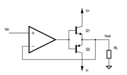
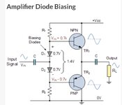
I am wondering if I have an OpAmp which can deliver maximum output current for example 50 mA and the output voltage across the load is -3 V and I need around 200 mA load current with -3 V. I found an approach to get higher output current then OpAmp. This can be done using two transistors but I am not able to understand how it work. Can someone please describe how the two transistors in the attached circuit work to get higher current ?
 

Attachments

  • Untitled 616.png
    Untitled 616.png
    26.8 KB · Views: 40
Thats an over simplified circuit to use as booster, but essentially Q1 is used to source
current, Q2 to sink. Here is an LM741 output stage, corrected for crossover distortion and
implementing current limit to protect it. But its low power, shown to equate the architecture
of your NPN PNP pair for power boost, eg same principles. It works because the high G loop
of an opamp drives output to meet its fdbk constraints, within spec affects like G and BW
and DC errors.

1708706825169.png


You can buy power boosted opamps,


Regards, Dana.
 
Last edited:
I am sorry. I am not able to understand the way you explained.

Can you please read the post and comment again ? Thanks in advance.
 
It's going to add crossover distortion but will throw whatever
current the load wants, once you slew the booster input to
the point that either E-B junction lights up. There are better
local configurations which will reduce the dead band and
improve crossover distortion. Realize that this booster will
defeat internal current limiting (which may be the actual
problem w/ bare op amp).
 
Here is a simple sim, where load is taking ~ 450 mA when G = 10 OpAmp
circuit goes to either + .5 or -.5.

You can see the current in the output transistors as well as the drive V
to their bases.

See the region on base drive, red curve, where Op[Amp out is ~ 0V, and its
G slope changes for a few mV from its nominal circuit setting of 10. Thats classic
crossover distortion, due to Vbe of the transistors to turn on, and can be mostly
eliminated with additional bias circuitry, as is done inside most opamps with
their output stage design.

1708720761289.png


Regards, Dana.
 
In device terms, Ebers-Moll, first order
1708739485813.png
where the controlling
parameter is Vbe. There is an industry ongoing forever debate I would add, is a transistor
a V or I controlled device. Its V controlled although current controlled model is quite
simple and effective in design. Until you get to extremely small geometry transistors.

But again OpAmp is looking at Voltages as the prime control loop, and
drives Vbe of the transistors to get the desired Voltage at the load R.

The way to insight is to write the equations KVL and take limits as G (internal OpAmp G)
gets very large simplified results and insight will get you there. But using V controlled
model for the Transistors makes this a trial by file......

There is much deeper insight that will give you migraines if you solve the
field equations in the silicon structure, which will make you look for a bridge to
jump off.

The main take away is the high G of the OpAmp drives the control loop to
set Vout = - G x Vin, and the external transistor provide the higher current needed
to drive the large load (low Rload) to that value.

Regards, Dana.
 
Last edited:
In simple terms just an emitter follower yields Ie= beta Ib
If the emitter voltage follows the base by a fairly constant Vbe, we know that the impedance ratios load to source are being satisfied by the Vbe controlled current at the desired slew rate.

The error amplifier must be fast enough to satisfied this requirement. It already has at least 1 or 2 emitter followers inside to achieve say a 20mA limit to lower the output impedance.


Even the Ebers Moll model does not include GBW or ESR effects of the dielectric interfaces in semiconductors in all conditions.

Yet, we can model it easier just like DC gain “hFE”. and AC gain “Hfe”to follow your input signal with limitations.
 
@engr_joni_ee, we digress. Do you see that essentially the external transistors
are replicating the internal OpAmp output stage but with greater current capability
in their die construction, ie. power transistors versus small signal transistors current
capability ?

W/o getting too complicated when you boost a OpAmp output this way you can have
stability issues depending on nature of load, such as if its capacitive. Thats a whole
other discussion but essentially boils down to adding zeroes to loop response to
effectively reduce phase shift due to poles, internal and external, until loop gain is reduced
to < 1 when phase shift = 180 degrees thru the loop (added to OpAmp thru inverting input
adding 180 degrees due to its sign change). A phase shift total thru loop of 360 degrees
with a loop G >= 1 generally produces the following effect (below). Tons of info on web
on this topic.. That analysis is fairly simple thru s plane (LaPlace) analysis/algebra.

1708774351105.png


OpAmps are a whole world of fun to work with/analyze/use and are now ubiquitous in
design work, as are micros. Many micros now have 1 or more OpAmps onchip to signal
condition such things as onchip A/D's.......to create G blocks, to use as filters, to transform
signal properties, to manage non linear sensor behaviour........application areas simply huge.


Regards, Dana.
 
Last edited:
Thanks for comments. I understand the concept of cross over distortion in push pull amplifier i.e., if the input to the base of the PNP and NPN in push pull amplifier is between +0.7 V and -0.7 V, none of the transistor will conduct.

I would like to explain bit more the actual problem in connection to post #1.

We have a DAC that is driven by an FPGA. The DAC is outputting variable 0 V to 3 V. We need to invert it. We already are using an op-amp in inverting configuration with unity gain that invert the polarity and gives 0 V to -3 V at the output of an op-amp. The op-amp we already have selected and for some reason we can not change the op-amp. The problem is that the op-amp is rated up to 50 mA output current and we need 200 mA through the load with variable negative voltage 0 V to -3 V.

The output of the op-amp will never be positive because we invert the output of the DAC using op-amp in inverting configuration. The output of the op-amp will be varing between 0 V to -3 V.

I was thinking to use push pull amplifier stage using PNP and NPN at the output of the op-amp as shown in the post #1. I guess in order to overcome the crossover distortion there are two solutions.

1- I can permanently bias both the base of transistors PNP and NPN using resistors and diodes so that both transistor always conduct.
2- Drive DAC to get 0.7 V to 3.7 V instead. The output of the inverted op-amp will be from -0.7 V to -3.7 V. And the push pull stage will give 0 V to -3 V.

Kindly suggest which option is better.

A question about push pull amplifier. In worst case, if the input signal is between +0.7 V and -0.7 V, and there is no diodes to turn the transistors on all the time. This is the case when none of the transistor will conduct. What will be the output when none of the transistor conduct ?. In our case, we can accept 0 V at the load which is not a problem.
 
Last edited:
What OpAmp are you using and what is its supply values ?

Historically one does what you mention in 1) above. Burns some power but
easy way to implement.


2) above compromises DAC dynamic range, otherwise doable.

If you google "class ab design power booster" no shortage of papers and design
ap notes.

A question about push pull amplifier. In worst case, if the input signal is between +0.7 V and -0.7 V, and there is no diodes to turn the transistors on all the time. This is the case when none of the transistor will conduct. What will be the output when none of the transistor conduct ?. In our case, we can accept 0 V at the load which is not a problem.

Keep in mind they are not completely off, nor are they matched pairs (typically)
so some current does flow to load. Last time I did one was 50 + years ago and
was focused on Tr and Tf in a f() generator application, so I forget how much offset
my case produced. Could not have been much as it was a 50 ohm system. Its basically
tiny leakage currents occurring.


Regards, Dana.
 
Last edited:
What IC is used ?
Is the load resistive?
What rise time and fall time do you need?
The transistors will always conduct when ever there is an error on the input of >0.6/Aol *Av i.e. microvolts.
Can you define the load better than -3V 200 mA ?

IS there a need for an NPN since as you stated Op Amp will always be negative, unless you have a non-linear or reactive load and need a fast rise time.
 
Nothing has been said yet about signal speed and dynamic accuracy requirements. We simply don't know if cross-over distortions are a problem and if the suggestion to eliminate it are relevant here.
 
In our case the input signal is changing is very very slow. Most of the time we need a stable output but at variable levels controlled by the DAC slowly changing.
 
Sounds to me as the originally discussed circuit is just perfect. Due to unipolar output, there's probably no crossing of current polarity at all.
 
NPN (with negative polarity supply at the emitter leg) can accept positive polarity bias voltage, and give you range of 0v to -3v to load.

Simulation: 3-bit counter outputs zero to +3V through binary-weighted resistor network. Experimentation results in a bias network that yields linear performance. Notice 8 distinct volt levels.

convert positive polarity count up to negative polarity 220mA (via NPN -3v supply).png

--- Updated ---

Link to run above schematic in Falstad's animated interactive simulator:

tinyurl.com/24k9nd83

Toggle Full screen (under File menu).
Drag upward on border of scope traces.
 
Last edited:
Hi,

The circuit in post#1 shows a class B outptu stage.
The known disadvantage is the "gap" where both BJTs are high ohmic |V_BE| < 0.5V.

I recommend to use a resitor between OPAMP_Output and the emitters of the BJTs.

Klaus
 
The ques using #18 circuit is how accurate does OP want the output V to be ?
Given its not in a error correction loop, NPN to NPN device variation,
T, DAC loading effects.......how many bits is it in the FPGA..... Need to
do a complete error budget.

FPGA dac PWM based or ladder......buffered or not ......?

Of course the following circuit in an OpAmp control loop can resolve most of these
errors.....

1708859560467.png


Regards, Dana.
 
Last edited:

LaTeX Commands Quick-Menu:

Part and Inventory Search

Welcome to EDABoard.com

Sponsor

Back
Top