Continue to Site

Welcome to EDAboard.com

Welcome to our site! EDAboard.com is an international Electronics Discussion Forum focused on EDA software, circuits, schematics, books, theory, papers, asic, pld, 8051, DSP, Network, RF, Analog Design, PCB, Service Manuals... and a whole lot more! To participate you need to register. Registration is free. Click here to register now.

High Speed High Voltage Level Shifter

Status
Not open for further replies.

ngmedaboard

Member level 3
Joined
Feb 7, 2010
Messages
60
Helped
7
Reputation
14
Reaction score
4
Trophy points
1,288
Location
United States
Activity points
1,831
To the board:

Objetive:
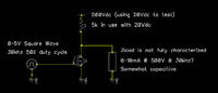
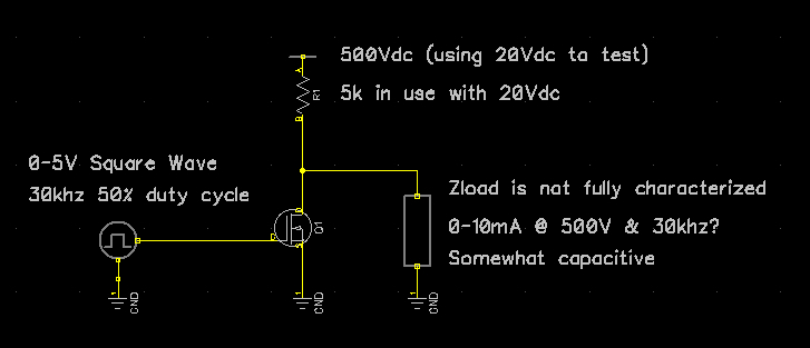
We looking to build an AC power supply with the following characteristics:
Voltage: 500V pk-pk
Waveform: Square
Duty Cycle: 50% for now
Frequency: 30Khz
Load: 0 - 12mA RMS somewhat capacitive
Note: We are currently testing the circuit open circuit so the load is not a factor in the problems currently being encountered. I have merely mentioned it as any design solution should not preclude the ability to supply the above mentioned currents.

Challenge:
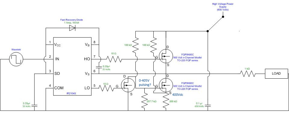
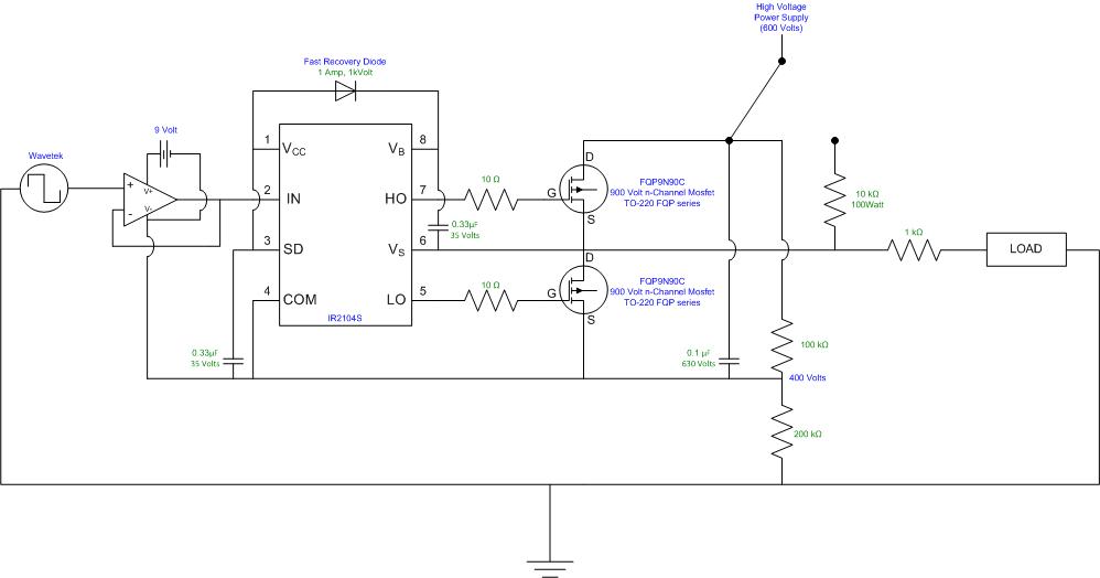
We don't currently have an AC supply or amplifier so are looking to construct a level shifter circuit. We have a high voltage DC supply, function generator and high speed high voltage switching FET **broken link removed** and have come up with the following approach which has not worked as well as we had hoped.


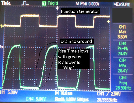
The biggest problem we have noticed is that if the resistance connecting the power supply to the drain is too high or in other works Id is too low, the rise time of the FET begins to suffer dramatically. Of course this only increases as the frequency is pushed beyond 1khz and up towards 30khz.
My prior experience with FETs has never led me to believe there is any benefit to their switching characteristics from increasing Id and thus I'd like to ask what might be happening hear that I am not considering?
I had anticipated my resistor selection here to be merely a factor of the DC supply voltage and my desired load current.

The following is a graph of what we're seeing with only a 20Vdc supply, a 5k resistor open circuit (no load). It's not terrible but you can already see a slow rise time.

77_1295810410.jpg


Any additional thoughts or recommendations are greatly appreciated.

---------- Post added at 21:24 ---------- Previous post was at 20:33 ----------

I'll note that we also poked around quite a bit looking for any stray capacitance that could have been in the circuit and couldn't find anything.

---------- Post added at 21:36 ---------- Previous post was at 21:24 ----------

Also thought about using a push pull arrangement but don't believe we had much luck finding a complimentary pair of FETs rated for the voltages in play here at least not for a high speed application. I suppose it could be done using a push pull pair with a step-up transformer on the output, but we'd like to avoid the need for a transformer if the more basic level shifter is possible.
 
Last edited:

The following is a graph of what we're seeing with only a 20Vdc supply

The graph is missing.

I have also noticed that you are driving the mofget with a gate voltage of 5V, i don't know your mosfet but maybe you can get better results with higher Vgs.

You have the load connected from the drain to the output, maybe you can try to use it in series between the drain and R1.

Alex

---------- Post added at 23:13 ---------- Previous post was at 23:08 ----------

I just saw that you have included the mosfet in your post,
the Rds(on) is rated 1.4 ohm for Vgs of 10v, i think you should try with a higher gate voltage.

Alex

---------- Post added at 23:19 ---------- Previous post was at 23:13 ----------

Actually the 5v that you are using are the max gate threshold voltage (3v-5v), you shouldn't use such a low voltage.

Alex
 

If the max Vgs threshold is 5V, shouldn't it be fully enhanced at that voltage? Yes, I believe the absolute Vgs rating is 30V but that's only to handle fault conditions. The gate voltage is spec'd for 5V max under normal operation. I mean theoretically you might obtain a lower Rds on by going above 5V but any gains I suspect would be asymptotic and I'd expect Rds to be low enough at 5V given the ratings.

Am I missing something?

-ngm

---------- Post added at 22:39 ---------- Previous post was at 22:38 ----------

Ah, and it shouldn't matter. This is an inverting level shifter. So the output only goes high when the FET is off. My issues are when the FET is off, not when it is enhanced.
 

Since your problem is only when switching off I assume that the problem isn't the gate voltage.
I see in the datasheet that the capacitance increases when the Vds gets lower,
I don't know if this creates any problem with you mosfet driver capability but it would probably show also in the turn on rising time and you say that the problem is only in the turn off speed.

mosfer_cap.jpg

Alex
 
I have made a few simulations, it seems that with any mosfet when the drain resistor (load) gets higher the turn off time gets slower,
I think that this has to do with a mosfet capacitance and because of the high resistance you get a high RC time.
When switching on the low resistance path (DS) gives a fast turn on.

Alex
 
Unfortunately, you didn't report the observed rise time. The drain node capacitance as such would result in at least several µs rise time, don't know if this is fast or slow from your point of view. You also can get small signal FET's with about factor 10 lower output capacitances. But for fast switching, there's no alternative to push-pull. Most likely all NMOS with floating gate driver.
 
Here's the scope picture for anyone that had trouble viewing it.

100_1295835585.jpg


---------- Post added at 03:25 ---------- Previous post was at 03:19 ----------

alexan_e I suppose we could look at Vds on another channel and see if there's any correlation with the capacitance. With the FET off that Vds is quite high...

Assuming that's the problem do you think adding a load would actually help this? I'm thinking that would help drain the capacitance and drop Vds down to 0 much faster. Does that make sense to you?

---------- Post added at 03:33 ---------- Previous post was at 03:25 ----------

Well in the example in the scope shot with 20Vdc on the power supply and 5k, no where near what we're shooting for rise time was about 13us.

Getting back to push pull, so you're suggesting that approach is necessary with a complimentary pair and that a single low side switch is insufficient at 30Khz? Again I think I'd then have to use an output transformer (step with low reactance) to hit the 500V pk-pk that we need. Do you agree with Alex that the problems we're facing stem from capacitance between source and drain in the FET? Any way to tune that out with some kind of LC network?

In terms of the floating gates where you thinking the idea that this needs to be AC coupled so that my low side FET is can be referenced below GND? I could also theoretically obtain the isolation with the output transformer as well couldn't I?

---------- Post added at 03:41 ---------- Previous post was at 03:33 ----------

I take back some of my comments to a complimentary pair push pull. I think that would only be of benefit if I were looking to produce an output that swings below 0V. I'm only looking to swing from 0 to 500V not -500V to +500V.

---------- Post added at 03:59 ---------- Previous post was at 03:41 ----------

What about using an N-FET level shifter simply to amplify my current capability and perhaps a add a little voltage. But instead of going for high voltage at that stage, I use the FET to switch a more hefty current (which seems to improve things anyway). But tack on a flyback transformer to get the HV rather than trying to drive HV directly from the FET.

Can I expect to get a decent waveform out of that at 30Khz with the right flyback transformer?
 

The waveform will get most likely worse with a load. (It's just a guess, because you didn't disclose any information about it).

Rise time is simply a matter of drain node capcitance (Cds + Cdg + Cload + Cprobe + Cstray) and Rload. The rise time of about 7 us shown in your screenshot is higher, than expectable by the FET capacitance only (2.2*5k*250pF), but basically normal operation for a single ended output.

The fall time is mainly limited by the inappropriate low gate voltage, as mentioned by Alex. 10 - 15 V would be reasonable for a standard (not logic-level) FET. My suggested simple push-pull circuit would be a HV bootstrap driver, e.g. IR2104 with two NMOS FETs.

If you don't have particular requirements for the output waveform, a transformer may be a solution. Otherwise you won't enjoy it.
 
FvM, beautiful! The IR2104 looks like what we need. Excellent! I've used similar drivers before, they can be nasty when they fail (i.e. turning on both FETs simultaneously), but for this application I'm not too worried. We'll probably give this approach a shot. It's simple and should work without any exotic mods!
 

Any reason you can't use a step up transformer for the output? Having all your switching done at low voltage then stepping it up would make things a lot easier, I imagine.
 

Well we were talking about that but FvM suggested it might impact the quality of our square wave. And I suspect depending on the transformer selected the characteristics of the load, reactance could become a problem and distort the wave further by turning this thing into a bit of a boost converter circuit (which is not the intention).

With that said, we may need to go past 600V, so we may still need to look at using an output transformer, but certainly not one with a significant turns ratio like a fly back. Probably a 1:2 step up at best which hopefully wouldn't be nearly as much of a risk to distorting the waveform.

Thinking out loud here. Anyone feel free to challenge or confirm my thought process.

Thanks
 

If you really want to stick with just solid state output, then you might want to switch from mosfets to IGBTs. They tend to do better at very high voltages. Also there is a bootstrapping gate driver rated up to 1200V: the IR2213. It's somewhat difficult to find for sale, though.
 
Also there is a bootstrapping gate driver rated up to 1200V
In addition, there are other options to transfer the control signal across an isolation boundary, e.g. pulse transformers, high speed opto coupler.

Regarding the output transformer question, it's possible of course. But I didn't yet hear a specification for the output waveform. And most people underestimate the issues with designing good high voltage pulse transformers.
 
In addition, there are other options to transfer the control signal across an isolation boundary, e.g. pulse transformers, high speed opto coupler.

FvM, I thought about something similar (using a voltage divider) but realized the pin used to sense the voltage between the two FETs is also used as the source connection to the upper N FET and thus needs to be connected there to turn on that FET. I think you'd have the same problem using an optocoupler, isolation transformer or AC coupling.
 

I tried the IR2104 and it is working great, based on the reference circuit in their datasheet. With that said, we want to look at pulsing between 400V and 600V instead of 0 to 600V. I was thinking about pulling up the the output to 400V and disconnecting the lowside FET, however I suspect that will complicate gate driving from the IC as one would need 405V to drive the gate of the high side FET.

Any ideas or comments on the complexity of being able to do this?

Thanks
 

Switching between 400 and 600 V imples a sufficient low impedance 400 V source (maybe a bypassed voltage divider in some cases, depending on the load current), and a floating (respectively stacked up the 400V source) supply for the gate driver.

The alternative for "switching" arbitrary voltages would be class A or AB high voltage linear amplifier.
 
FvM, yes our thoughts are along the same lines. We came up with the approach that we'd create a 400V source with a divider off of the 600V supply (let's assume the 600V supply is sufficiently low in impedance while the load is sufficiently high in impedance). And that would feed the source of the low side FET rather then ground. To turn it on, I was thinking we use a level shifter to put the needed 405V on the gate of the low side FET (fingers crossed this won't add enough propagation delay to screw up the phase alignment). Much thanks if you could look over this concept and offer your comments (waiting on parts to actually build it).


if you could look over this concept and offer your comments
It can't work this way. Two points are missing:
- bypassing of the 400 V voltage divider
- restricting the gate voltage to the permissible range

The shown circuit would immediately blow the gate of the low-side FET by applying -400V to it. Whatever you use to adjust the correct voltage range, you should have voltage limiting means to enforce keeping of the maximum values. Unfortunately most gate driver and voltage limiting circuits will feed a current into to 400V supply, so a high resistance divider most likely isn't a good idea. A divider with a source follower would give a less compliant voltage source. Capacitive bypassing to absorb the switching currents would be required anyway.

I fear, you also didn't yet realize, that the boostrap circuit relies on switching the output to ground, which isn't longer the case now. But you would be still able to use an IR21xx driver, if you power it by a fixed supply stacked up above the HV.

You didn't - by the way - mention the involved load impedance.
 
Oh, you're right! I'd be pulling the gate of the low side FET below it's source! to the tune of -400V

The load impedance is very high but not fully characterized (that is part of the experiment), I can say that is somewhat capacitive, but the bootstrap topology has helped dramatically in terms of overcoming the challenges associated with a capacitive load. With a 0 600V wave 50/50 duty cycle, we were seeing this load pull less than 10mA RMS.

I need to think on your comment regarding the stacking of the IR driver over the HV supply. We noticed that the chip seems to phantom power itself without even suppling Vcc for some reason. Seems to work well whether we power Vcc or not.
 

I'm also working on this project, and earlier today I hit my head on the bathroom sink while trying to hang a clock and I had an idea:

What if a 741 op amp was used to separate the function generator from the IR2104 chip, and the op amp, chip, and low side mosfet were all common at a high voltage set by a divider. See attached image.

I've done similar things with op amps, but I have a feeling i'm missing something. Any thoughts???

---------- Post added at 17:23 ---------- Previous post was at 17:23 ----------


Status
Not open for further replies.

Part and Inventory Search

Welcome to EDABoard.com

Sponsor

Back
Top