Continue to Site

Welcome to EDAboard.com

Welcome to our site! EDAboard.com is an international Electronics Discussion Forum focused on EDA software, circuits, schematics, books, theory, papers, asic, pld, 8051, DSP, Network, RF, Analog Design, PCB, Service Manuals... and a whole lot more! To participate you need to register. Registration is free. Click here to register now.

Hi side drive level shifter problems?

Status
Not open for further replies.

cupoftea

Advanced Member level 5
Joined
Jun 13, 2021
Messages
2,659
Helped
54
Reputation
108
Reaction score
116
Trophy points
63
Activity points
14,000
Hi,
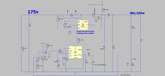
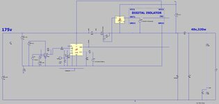
The attached shows a Hi side drive level shifter. (LTspice and jpeg scm) Ignoring its voltage rating, do you see problems with this set-up?
In the actual circuit , we would use a 2ED2182S06 Bootstrap drive chip instead of LTC4440.

The problem here seems to be that the "TS" pin of LTC4440 has to go >100V below the "GND" pin. Would you agree? This also would be a problem with 2ED2182S06?

LTC4440

2ED2182S06
 

Attachments

  • Buck hi side drive.jpg
    Buck hi side drive.jpg
    139.4 KB · Views: 80
  • Surge Buck_level Shift_230113.zip
    2 KB · Views: 73

Thanks, as can be seen , unfortunately its more than a transient, it goes to well below -100V in "normal" operation.
I am amazed it cant put up with this....it can handle such high positive voltages, but not as high negative voltages
 

I don't see a way to get -100V in the shown schematic. Are you talking about different circuit?

In any case, repetitive negative voltage isn't compatible with bootstrap operation principle. Need to go for DC/DC converter.
 
Thanks, if you were to run the sim of the top post, you would see to what i refer.....the TS pin goes well more than 100V below the GND pin of the LTC4440, when the FET switchs off and the buck diode conducts. It seems odd that this is a bad thing, when ot can easily handle TS pin going well above GND (ie more than 100v above it, in the case of 2ED2182).
--- Updated ---

We wonder about using the attached?...
 

Attachments

  • Buck hi side DigiIsolator drive.jpg
    Buck hi side DigiIsolator drive.jpg
    131.5 KB · Views: 77
  • Surge Buck_DigiIsolator_230113.zip
    2.1 KB · Views: 84
Last edited:

I finally realized that you intentionally isolated bootsrap driver ground in post #1 circuit. That can't ever work.

I couldn't imagine you'd connect a bootstrap driver in this weird way.
--- Updated ---

Regarding other design with isolator, it's still not operational because at least Vdiv feedback isn't designed correctly, output is ground referenced while LT1243 is floating. Not sure what you are specifically trying to achieve.
 
Last edited:
Regarding other design with isolator, it's still not operational because at least Vdiv feedback isn't designed correctly, output is ground referenced while LT1243 is floating. Not sure what you are specifically trying to achieve.
Thanks yes, you are entirely correct, though that part of the circuit we can take care of.....so please just "pretend" that bit is taken care of by magic for now.

It is the driving of that NFET from the controller which is grounded to the place where you can see it grounded. We need a way to refer that controllers gate drive signal to the NFET as shown.
I think also a UCC23513 digital isolator could be used?
I think totem pole PFCs do this kind of thing as they very often have controllers referenced to the hi side?

UCC23513
 

Actually, the NCD57201
...purports to be able to handle VS (switching node) pin going +/- 800v either side of chip "proper" ground.

I find this hard to beleive, ...if it were capable fo that, then it would have wiped all the other bootstrap drivers off the market?
 

Bad Jinglish, it means the Vs can handle an 800V swing, i.e. when the bottom device is on Vs is -800V compared to when the upper device is on ....
 
NCD57201 spec is clear about allowing +/- 800 V between Vs and GND (LS source). It uses true galvanic isolation for HS control signal instead of a level shifter. In so far it's clearly different from usual IRF bootstrap driver chip and successors. If you are using bootstrap supply through diode, the negative voltage must be nevertheless limited to short transients, absorbed by a series resistor. But with isolated supply as in post #1, the negative voltage can be applied statically.
 
I fully expect -800V to make it go pop .....
--- Updated ---

although, to be fair the data sheet does say -800V more than once

time to buy some and test ....
 
Last edited:
I have no doubt that NCD57201 is designed for +/- 800 V rating of the built-in isolator

1673854456628.png


In typical applications, it's not suited for > 160 V working voltage due to 0.8 mm creepage between LO and VS pin though. You'd need to mold the IC for higher continuous voltage rating.

Curiously the datasheet is reporting an external creepage of 4 mm (the distance between left and right pin row), simply forgetting that LO carries also low side potential.
 
Status
Not open for further replies.

Part and Inventory Search

Welcome to EDABoard.com

Sponsor

Back
Top