Tetik
Member level 5

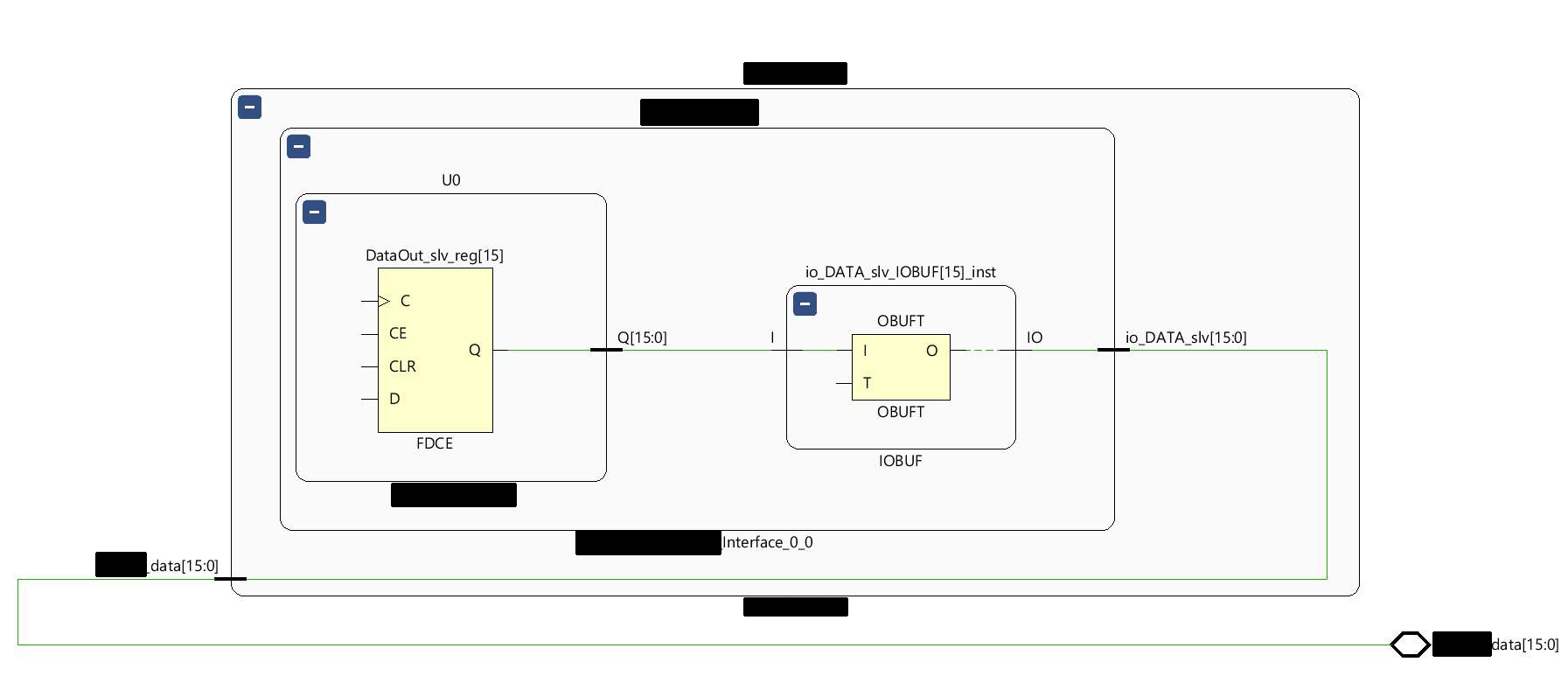
I have a chip connected to my FPGA which provide the clock with the bidirectionnal data bus. The clock frequency is 100MHz. Here's a view of my implementation for the dataout from the FPGA to the chip.

The clock of U0 is connected directly to an IBUF and BUF. After my implementation, I have a timing error. The source clock path (pin->ibuf->bufg->C) is about 5.140ns and my datapath (FDCE->OBUFT->pin) is about 7.0ns. The total delay is higher than the allowed 10ns.
What are my options here?
Do I have to use a MMCM to eliminate the source clock path (phase shift)?
Can I just ignore the source clock path and how to specify it in the constraints file?
Any other options?
For the info, the FPGA is the master of the bus and provides the control signal of the interface but the clock comes from the external chip.
Any help please.
