Continue to Site

Welcome to EDAboard.com

Welcome to our site! EDAboard.com is an international Electronics Discussion Forum focused on EDA software, circuits, schematics, books, theory, papers, asic, pld, 8051, DSP, Network, RF, Analog Design, PCB, Service Manuals... and a whole lot more! To participate you need to register. Registration is free. Click here to register now.

Help with modifying this opmap circuit

Status
Not open for further replies.

floppy32

Member level 1
Joined
Dec 5, 2019
Messages
40
Helped
0
Reputation
0
Reaction score
2
Trophy points
8
Activity points
363
Hello,

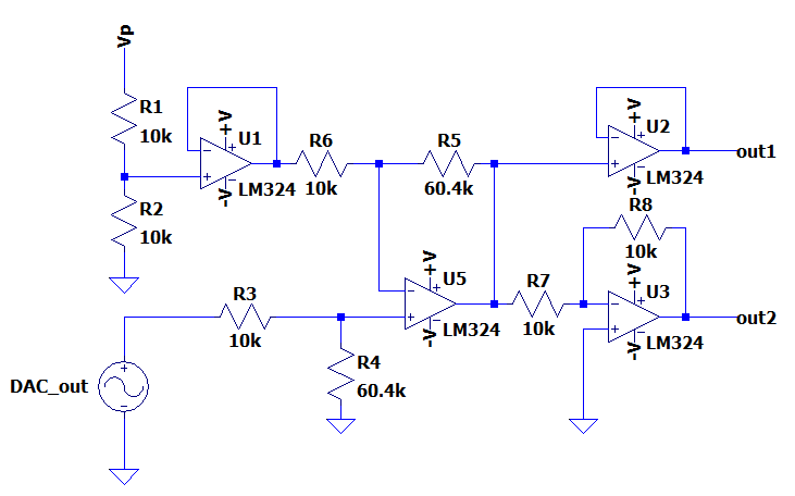
I have the following circuit which takes the DAC output as input and amplifies and creates bipolar output:
1650400098459.png


I have read that if DAC_out goes to the inverting input the CM noise would be better. Vp is supply voltage of the DAC.

Im no expert and need to use this circuit as interface.
Can someone help me to modify this circuit such that DAC_out will go to inverting input keeping the functionality same?
 

I don't know why you're worried about noise if you're using an LM324. There are MUCH better op amps available that aren't 50 years old. Further, putting those large resistors in the signal path also contribute noise. Further yet, why are you only concerned with common-mode noise? I think you're getting concerned about something that may not even be an issue when there are so many other sources of noise in your circuit. A non-inverting op amp has no resistor on the input, and therefor no resistor thermal noise. Non-inverting configurations as used all the time, although most higher-end DACs have a differential output.

Take a look at this.
Hello again, thank you for the paper. Where should I add the gain stage? I also want voltage gain of 2.

I modified it as follows:

1650403984641.png


What do you think would that be correct?
 

Eliminate U1 as its just unity G follower, driven by a V source with G,
outlined in red, so just set desired G there.


Regards, Dana.
 

Eliminate U2, not needed. And with proper design of bias network get rid of U1.

Or just 1 OpAmp (OPA320 not needed) -

1650415160445.png


Regards, Dana.
 
Last edited:

Hi,

I sometimes say: a circuit without capacitors is no circuit.

In your case ... where you talk about noise .. it's essential to use capacitors.
* for proper power supply bypassing: a bulk capacitor per rail and a ceramics capacitor at each power supply pin of each IC.
* as LPF to reduce noise at the (voltage divider of ) Vref
* as RC LPF at DAC output to reduce dV/dt to avoid Opamp overdrive
* as LPF at the signal output to omit high frequency noise

I agree all of the above reagarding low noise.
Also: I'd never use a supply voltage as Vref when I want low noise. Supply voltages are noisy.

Klaus
I have uC pins 3.3V and 5V which I use as Vref now. But what could be better to use in this case for Vref? A voltage regulator which regulates from opamp supply or a voltage regulator from uC supply? What component could Vref be?
--- Updated ---

Eliminate U2, not needed. And with proper design of bias network get rid of U1.

Or just 1 OpAmp (OPA320 not needed) -

View attachment 175581

Regards, Dana.
What opmap is this? I have LM324. But yours has inherently bipolar output pins. I also need DIP.
 

The OpAmp is Analog Devices, some dips at bottom of this selection tool :

https://www.analog.com/en/parametricsearch/11081#/

Your constraints of G = 2 (without throwing away G with input R divider) and DIP might make
choices slim.

What is your DAC Vout range ? Same for power supply for design ? Frequency range of DAC out or max sample rate of DAC ?


With regards to Vref there are a number of parts industry offers, search Digikey for the
parameters you want.

Regards, Dana.
 
Last edited:

The OpAmp is Analog Devices, some dips at bottom of this selection tool :

https://www.analog.com/en/parametricsearch/11081#/

Your constraints of G = 2 (without throwing away G with input R divider) and DIP might make
choices slim.

What is your DAC Vout range ? Same for power supply for design ? Frequency range of DAC out or max sample rate of DAC ?


With regards to Vref there are a number of parts industry offers, search Digikey for the
parameters you want.

Regards, Dana.
Hi again,

I couldnt find any DIP diff opamp with bipolar outputs. Can you see any?

In my application I use this SPI DAC module: https://www.mikroe.com/dac-8-click So it varies between 0 to 2.5V now with 3.3V Vcc from an uC board. And I need to produce bipolar outputs(Vp and Vn) from this DAC. I need -Vp- Vn vary from -10V to 10V. So I both need some gain and also produce bipolar outputs.

The final bipolar outputs will go into a galvomirror which has 6kHz filter. And I will vary the DAC in stair step fashion at each 600us. So Im mostly interested in DC and not disturbing DNL.

For the LM324 circuit now I use a bench supply at +/-12V for Vcc and Vee. I didnt male or buy a split supply yet for the circuit.

I hope its more clear now. But unfortunately I couldn't find a dedicated IC in DIP.
 

I went to digikey, lots of parts but PDIP is the killer. There is PDIP in the analog devices link
I sent, but power supply (too low for swing) is the limitation.

So you will have to do it with standard opamps, unless you used a SOIC to dip type adapter
board.


Regards, Dana.
 

Hi,

"I have uC pins 3.3V and 5V which I use as Vref now. But what could be better to use in this case for Vref? A voltage regulator which regulates from opamp supply or a voltage regulator from uC supply? What component could Vref be?"

Only you can know how precise you want/need Vref to be across expected temperature range and supply voltage fluctuations/ripple. I only understand you need a mid-supply reference, I do not know how fussy you are or how precise the circuit must be. I thought MCU regulated output voltages are rather imprecise and quite... let's say basic. Check the MCU datasheet to see how much the nominal '3.3V' is actually 3.300V (!) and how much it may change with temperature.

There's an argument for using the supply rail or MCU regulated output voltage and a resistive divider as Vref as then everything is moving around/up and down at the same level (unless there are terrible spikes on the supply line). This, again, only you can know what the circuit needs with regard to a reference voltage - precision or supply voltage synchronicity between components.

I wouldn't use a voltage regulator as a reference myself, especially as some people even use a voltage reference IC in an adjustable voltage regulator's feedback loop to fine tune the voltage regulator's 'imprecise' output voltage... In theory, at least: voltage regulator = coarse regulation; voltage reference = fine regulation.

TL431 is a simple to use adjustable part, but it drifts somewhat for my liking depending on what I am hoping to achieve. e.g. TL431C has an initial voltage at 25ºC = 2.440V min, 2.495V typical, 2.550V maximum, it can drift an additional 4mV to 25mV with temperature changes. I was surprised to see the LM4041 is far 'worse' than the TL431 with regard to temperature drift. There are many other voltage references that are far 'stiffer', you just have to do a parametric search.

If you don't feel like reading a lot of datasheets to see which voltage reference has the lowest ppm/ºC and initial tolerance or what load it can handle (irrelevant point as an op amp biasing device which will have tiny bias currents), or it's not important for your needs, try the TL431 (~2.5V), or TLV431 (~1.25V), for example - easy to use and importantly, the Spice, etc. models are widely available.
 

Status
Not open for further replies.

Similar threads

Part and Inventory Search

Welcome to EDABoard.com

Sponsor

Back
Top