Continue to Site

Welcome to EDAboard.com

Welcome to our site! EDAboard.com is an international Electronics Discussion Forum focused on EDA software, circuits, schematics, books, theory, papers, asic, pld, 8051, DSP, Network, RF, Analog Design, PCB, Service Manuals... and a whole lot more! To participate you need to register. Registration is free. Click here to register now.

Help me the holdtime problem

Status
Not open for further replies.

jjftt

Newbie level 6
Joined
Jul 24, 2007
Messages
11
Helped
0
Reputation
0
Reaction score
0
Trophy points
1,281
Activity points
1,335
In a flip flop like this,anyone can tell me how is the hold time violation come from?
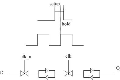
when clk=1,the first tran_mos is off, how can the input D effect the output Q?


89_1195739214.gif
 

can u pls put hte diagram bit more clearly ...
so that its easy to understand !!!
 

suppose the clk changes at the 2nd transistor before the clk at the 1st transistor (they will not change simultaneously). Also, suppose the D input changes just before clk->1.
 

sorry, i have redrawn the diagram.
when the clk=0, input d is stored in the first inverter loop. it need some time to go to stable before the clk=1, this is the setup time.
But how about the holdtime? when the clk=1,the first tran_cmos is turned off, why the input data d shoud be stable after the clk=1.
 

"But how about the holdtime? when the clk=1,the first tran_cmos is turned off, why the input data d shoud be stable after the clk=1."
I suppose that this is because of the propagation time that is required by the following combinational logic circuit.
 

Status
Not open for further replies.

Part and Inventory Search

Welcome to EDABoard.com

Sponsor

Back
Top