Continue to Site

Welcome to EDAboard.com

Welcome to our site! EDAboard.com is an international Electronics Discussion Forum focused on EDA software, circuits, schematics, books, theory, papers, asic, pld, 8051, DSP, Network, RF, Analog Design, PCB, Service Manuals... and a whole lot more! To participate you need to register. Registration is free. Click here to register now.

help me for this circuit

Status
Not open for further replies.

fengluan

Junior Member level 3
Joined
Apr 14, 2006
Messages
27
Helped
0
Reputation
0
Reaction score
0
Trophy points
1,281
Activity points
1,463
54_1165026886.GIF


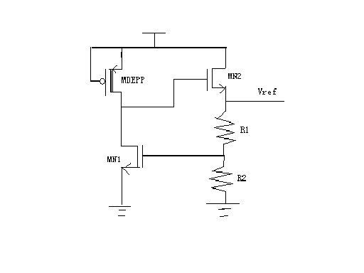
look at the circuit above,it's a voltage reference circuit. in my opinion, Vref=Vgsmn1×(R1+R2)/R2,and Vgs=Vth+........ Vth has negative TC and Id has positive TC .

i don't know whether i think is right. and how to analysis it's frequency responce.
 

if the gate voltage of MN2 is high,then the right path has no current.
the result you give is uncorrect,and this time,the MN1 have Vds>Vgs-Vth.
and the gate voltage of MN2 is low,so the result is right
 

VREF≡ SUPPLY VOLTAGE .
PMOS DEP = IS NOT OFF.
NMOS2 ITS GATE = NEARLY CONNECTED TO VDD
NMOS2 = NEARLY ON.
SO VREF=VDD.
PLZ MENTION THE REGION OF OPERATION OF ALL MOS .
YOU SET.
 

to fengluan, you are right.Vref=Vgsmn1×(R1+R2)/R2.Mdepp here acts as a current source,you don't need to do the the ac analysis actually since it is surely stable.Anyway, if you want to do,break the loop at the gate of Mn2
 

Status
Not open for further replies.

Part and Inventory Search

Welcome to EDABoard.com

Sponsor

Back
Top