Continue to Site

Welcome to EDAboard.com

Welcome to our site! EDAboard.com is an international Electronics Discussion Forum focused on EDA software, circuits, schematics, books, theory, papers, asic, pld, 8051, DSP, Network, RF, Analog Design, PCB, Service Manuals... and a whole lot more! To participate you need to register. Registration is free. Click here to register now.

Help! Can someone clarify to me how this converter circuit works?

Status
Not open for further replies.
Ok, thanks Genome. Maybe I'll try to test without the resistors or can I use a lower resistance?
 

I had tried..It seemed no difference. When I tried with higher voltage, the voltage drop is less. So, I think it should be ok. I would like to ask if a square wave signal after the two switches drop to negative. Is there any problem? Before the two switches, the output is DC so after the two switches, the waveform should be maxDC and zero. But I obtained +ve and -ve.
 

It depends on where you are measuring and what you have in circuit..


If you measure VA and VB then,


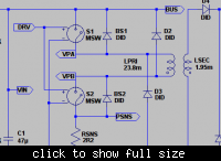
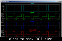
When DRV is high with the switches on then VA is taken to VBUS/311V by the upper switch and VB is taken to 0V/GROUND by the lower switch. When DRV goes low the switches turn off but current in the transformer primary magnetising inductance continues to flow and VA is driven down to 0V/GROUND and 'caught' by D3 becoming forward biased whilst VB is driven to VBUS/311V and caught by D2 becoming forward biased. During this time the transformer is reset. When magnetising current decays to zero VA/VB return to VBUS/2. In real life there will be ringing on the waveform.

If you measure between VA and VB then you will see something like the bottom trace and, yes, it would appear that the voltage has gone negative but that is the voltage 'across' the primary.

Genome.
 
Genome, where is the Va and Vb?

All components I connected them through breadboard and polystyrene. Now, I would like to test with higher voltage. Can a breadboard stand that? Or do I need to do PCB first? Can a normal PCB stand 240Vac?
 

Sorry, I meant VPA and VPB as labelled in the picture of the model across the primary of the transformer.

Have you received the parts I sent yet?

You really should have a PCB and it should be carefully laid out but perhaps you do not have time left to design one and get it made. I would not recommend a 'bread-board' if you mean one of those, solder-less, prototyping boards where you plug components into holes and your mention of polystyrene makes me worried that the thing will immediately not work and then burst into flames.

Do you have some vero-board?

VERO|01-0021|VEROBOARD 121.92X101.6MM | Farnell United Kingdom

Yes a normal PCB can withstand 240V AC. You just have to pay attention to clearances between tracks. If you do use vero-board then plan your layout first and be neat. Try to avoid placing high voltages on adjacent strips and break strips close to such points to avoid having such voltages all over the board.

Genome.
 
Yea I know the breadboard and polystyrene will no work out. I just test them at low voltage.

What is the Veroboard? It looks like strip board. Can it stand 240Vac?

Sorry, I still not yet receive the parcel. :sad:

---------- Post added at 04:56 ---------- Previous post was at 04:50 ----------

Haha..It is strip board. I just checked. If the components' legs are larger than the hole in the strip board, how to do it? Just drill a bigger hole?
 

It will be suitable for prototyping but as suggested it would be wise to avoid running high voltage on adjacent tracks. Yes.. I suppose if the legs do not fit then bigger holes would be needed.

Regarding the parcel that is frustrating. It was sent airmail 3rd March but I did not request any special service and Royal Mail are about as much help as an unhelpful thing other than claiming it should have taken 5 working days. Grrrrrr. I don't know what to do or suggest unless it has got delayed at customs, assuming it has not just disappeared down some wormhole...

I notice that you have a customs office at Sabah & Sarawak but, although it is close to you would not know if the parcel would have to pass through that particular location. Would it be possible for you to call them and ask if they have seen it..?

Genome.
 
sorry Genome for late reply.. I have asked. Do you have the registered number for the mail? Can you pm me the number?
 

I'm so so sorry. I have wasted your effort. I'll try go and ask again. From where you sent the parcel?

By the way, I would like to ask do I need heat sink for the mosfets for the circuit?

For the transformer to step down from 240V to 48V, you mentioned that the voltage will drop to 24V due to the 50% duty ratio. But my circuit, the output voltage does not drop so much after the transformer. When I tried with 47Vac, I let the circuit to run for some time, there is some noise. Will there be a problem? After I have the noise, the output voltage does not drop anymore. It is the same as the output voltage from the transformer.
 
Last edited:

For the 1 Ohm resistor, is 0.25W enough? i simulated the circuit..I see the current is quite high and the power loss is more than 0.25W.
 

I have checked..It is the capacitor's problem. However, when I tried with 42Vac, I can hear some noise. The noise is like "tik tik tik". Is it come from MOSFETs?
As for the 1 Ohm resistor, the current is about 1A with 42Vac.
 
Last edited:

I think the noise is come from the sparks. I do no know why when I connected the probe to the output capacitor, there are sparks. I think my component spoilt because the output voltage of the capacitor is same as the output of secondary transformer. It is weird.
 

Genome, do you think is the inductor problem? The output voltage from the secondary is normal. But I keep getting the capacitor voltage same as the secondary voltage. I left 1 week to complete the circuit. Please give me some suggestions.
 

Status
Not open for further replies.

Similar threads

Part and Inventory Search

Welcome to EDABoard.com

Sponsor

Back
Top