Continue to Site

Welcome to EDAboard.com

Welcome to our site! EDAboard.com is an international Electronics Discussion Forum focused on EDA software, circuits, schematics, books, theory, papers, asic, pld, 8051, DSP, Network, RF, Analog Design, PCB, Service Manuals... and a whole lot more! To participate you need to register. Registration is free. Click here to register now.

gm/Id method, where this comes from?

Status
Not open for further replies.

AMSA84

Advanced Member level 2
Joined
Aug 24, 2010
Messages
577
Helped
8
Reputation
16
Reaction score
8
Trophy points
1,298
Location
Iberian Peninsula
Activity points
6,178
Hi guys,

I've started studying the gm/Id method and I've already all the material needed (I think). I have just read 3 papers on this and I have a doubt.

I have seen some plots with the n factor.

Do anyone know what's this about and where or how can I get this variable?

I have managed to plot the gm/Id. Now I need to understand this n factor and the Inversion coefficient.

Regards.
 

Plus I watched the EE240 lecture from Berkley and they introduced a factor V* which from what I understood is the same as Vov. So what's the point of giving another name?
 

n factor is a characteristic coefficient and is explained in every book about semiconductor physics - it exists in I-V relationships of each diode, BJT, etc and varies for different materials.
 

Thanks for the reply Dominik.

The gm/Id method can be used to design comparators, current mirrors, level shifters, inverters, etc?

This method can be used to design circuits with the BSIM model? From what I have read, it was derived for the EKV model. What's the differences between this method applied to the EKV and BSIM?

Do you know how the IC is derived? Where it comes from? Where can I find that derivation, just to have an idea from where it comes from.

This kind of gm/Id method, from what I've understood was adopted to design circuits or at least amplifiers in newer technologies operating in weak inversion due to power supply restrictions. Something that I asked myself is: Is it possible to use this methodology to design the same circuits in strong or very strong inversion region?

In Binkley book you can see a picture (pag. 54) where he shows a Veff. What's veff? Vdsat? BTW Vdsat = Vov, correct? (there should be a fuc%"(&^g convention for the terminologies used in CMOS. Why is that the author says that we can get Vdsat negative?

Has someone watched the EE240 from Berkley? I would like to know why the used the V* and what it means. I didn't get it.

Regards.
 
Last edited:

EDIT: Forgot to ask another question. In other material that I've read, like EE240 or Murmann toolbox for gm/id, when they plot the gm/id they do it versus the Vov (Murmann) and V* (EE240) like mentioned above.

Why?

What's the difference between doing this approach and the one in the Birkley's book? Birkley's book is about the EKV model?
 

In other material that I've read, like EE240 or Murmann toolbox for gm/id, when they plot the gm/id they do it versus the Vov (Murmann) and V* (EE240) like mentioned above.

Why?
Because there's no standard designation. Every Prof. is used to his own.

What's the difference between doing this approach and the one in the Birkley's book?
You think of Binkley's book, I guess. Binkley uses the Inversion Coefficient (IC) instead of Vov, which is process independent.

Birkley's book is about the EKV model?
No, it's much more generally applicable.
 

1. gm/Id methodology could be used to design any kind of circuit but I don't want to categorically comment if it is the best way. But i can say that using this methodology You are able to develop optimal design working in every inversion region and this optimization be made faster and more accurately than using classic square-root equations in moderate/strong inversion (very strong inversion is not achievable in practice)

2. BSIM models in versions below 6 are developed from spice threshold voltage based models so they are non-physical and discontinuous on the edges of operating regions. The EKV model is based on physical quantities like other charge based models, but it approximates transfer characteristic of mosfet with quassi-empirical relations proposed in early '80s (if I good remember original paper was published in 1982 but I don't remember an authors names, maybe in origianl EKV paper from 1995 it should be cited). The better approximation is made in ACM model proposed by Cuhna et al. in 1998, which is based on Lambert W function (direct solution of charge sheet based mosfet model). One year ago I also found very nice paper about MOSFETs modeling (Microelectronics Reliability 55, 293–307), which uses poly-logarithm functions approach, which also is good approximation (but like used in EKV still "non fully physical") and from analytical point of view is a grateful approach because any integration or deriveration of poly-logarithm functions changing it order only.

All above approaches results in slightly different gm/Id curve shape which differences are still acceptable due to approximation errors made in models assumptions.
Of course we can still using BSIM3/4 models to subtract a number of coefficients required by gm/Id methodology (also same gm/Id curve is very close to reality).

3. In every case IC is derived as saturation current normalized to technology current which is similar in all above models but could be achieved in a slightly different ways.

4. The confusion with Vov, Vdsat and V* voltages is related with their similarity and results of classic spice/square-root threshold voltage based approach in which all of those three voltages are equal.
Vov is threated as difference of gate-source voltage to threshold voltage which is non-physical parameter but it is commonly used due to it simplicity and rooting in all generations of electronic engineers. V* also named Vp is a pinch-off voltage which also could be derived, in relation to threshold voltage, from transfer characteristic.

I think the quite easy explanation of all issues controversial for You is in P. Jespers book "Gm/Id methodology…".
I have also some words about modeling in my PhD thesis but I was too lazy to written it in English so it is useless for You ;-)

In my work I usually simplifying my life by assuming that pinch-off voltage is equal to overdrive one, applying short channel effects into current gain factor (if any) and using all of this hand made solutions only as starting point.
 
Because there's no standard designation. Every Prof. is used to his own.

But all of them means the same?

You think of Binkley's book, I guess. Binkley uses the Inversion Coefficient (IC) instead of Vov, which is process independent.

Yes I was referring to Binkley book. Yes he uses the IC, but this parameter is associated to the EVK model, correct? I ask that because the idea that I retained was that the IC is a parameter that is used for the EVK model and if that's true why there are people using V* and Vov or Vgs-Vth? They are adulterating the foundation, no?

But on another hand, for example Jespers in his gm/id book, he explains this methodology based on t he EVK, riht? Correct me if I am wrong, because that's the idea that I retained. But controversially in one paper that he has his name: gm/id methodology applied to an OTA they use the gm/id vs ID/(W/L) which is odd and they doesn't mention the IC or maybe the I(square picture) in the paper is meant to be the IC.

From what I am aware of, people that teach analogue design are trying to push this methodology but there is no sufficient material and specially clear material with good explanation which is ridiculous.

No, it's much more generally applicable.

Do you think so? Why is that on those slides that I mentioned above, teachers don't use the IC? And if we look to this IC expression for example, there is a I0 there that is specifically to the process but I have read here in the forum somewhere that this parameter is not given by the foundry. How's supposed we get that parameter for example?

Going back to jespers book for example, he has a Id = gm / (gm/Id)*. What's supposed to mean the *? Then he jumps to the next expression saying that W = (W) * Id /(Id)*. Whata heck this means? Geez.

- - - Updated - - -

1. gm/Id methodology could be used to design any kind of circuit but I don't want to categorically comment if it is the best way. But i can say that using this methodology You are able to develop optimal design working in every inversion region and this optimization be made faster and more accurately than using classic square-root equations in moderate/strong inversion (very strong inversion is not achievable in practice)

But why you don't want to comment it? Is there any detail that is missing on the literature?
By the way, you are saying that this methodology can be valid for every inversion region. But like I mentioned above to erikl answer, this "every inversion region" is supposed to be for the EVK model right? Because from what I have read the BSIM model is not valid or there is no model for the moderate inversion.

So we hit the same button. This methodology was developed for the EVK, how this can be adapted to the BSIM model? Who did this, or started to adopt this methodology for the BSIM model is adulterating the process, no?


2. BSIM models in versions below 6 are developed from spice threshold voltage based models so they are non-physical and discontinuous on the edges of operating regions. The EKV model is based on physical quantities like other charge based models, but it approximates transfer characteristic of mosfet with quassi-empirical relations proposed in early '80s (if I good remember original paper was published in 1982 but I don't remember an authors names, maybe in origianl EKV paper from 1995 it should be cited). The better approximation is made in ACM model proposed by Cuhna et al. in 1998, which is based on Lambert W function (direct solution of charge sheet based mosfet model). One year ago I also found very nice paper about MOSFETs modeling (Microelectronics Reliability 55, 293–307), which uses poly-logarithm functions approach, which also is good approximation (but like used in EKV still "non fully physical") and from analytical point of view is a grateful approach because any integration or deriveration of poly-logarithm functions changing it order only.

All above approaches results in slightly different gm/Id curve shape which differences are still acceptable due to approximation errors made in models assumptions.
Of course we can still using BSIM3/4 models to subtract a number of coefficients required by gm/Id methodology (also same gm/Id curve is very close to reality).

So you're saying what I have commented above, this methodology applied to the BSIM is adulterated and doesn't produce the same results as the ones we see in the Binkley book and Jespers book. They treat the examples and data as if they were using the EVK which is useless because almost nobody in the industry uses this EVK model so their books are useless into certain extend.

3. In every case IC is derived as saturation current normalized to technology current which is similar in all above models but could be achieved in a slightly different ways.

This IC cannot be obtained for the BSIM, right? So it's useless speaking about it.

4. The confusion with Vov, Vdsat and V* voltages is related with their similarity and results of classic spice/square-root threshold voltage based approach in which all of those three voltages are equal.
Vov is threated as difference of gate-source voltage to threshold voltage which is non-physical parameter but it is commonly used due to it simplicity and rooting in all generations of electronic engineers. V* also named Vp is a pinch-off voltage which also could be derived, in relation to threshold voltage, from transfer characteristic.

Well the confusion here I would say is that in all the xpto guru's books they speak about the IC and they use it in their plots and explanation blabla but at school, picking the example of Berkley EE214 they use Vov. Wtf? So we can do whatever we want, adulterate the foundation of the model but without explaining how why what?

Where did you read or heard that V* was the pinch-off voltage?

I think the quite easy explanation of all issues controversial for You is in P. Jespers book "Gm/Id methodology…".

Yeah, I have this book but it's completely poor written and the material is vague. The author thinks that we are inside his head.

I have also some words about modeling in my PhD thesis but I was too lazy to written it in English so it is useless for You ;-)

Nowadays every PhD is written in English :p

In my work I usually simplifying my life by assuming that pinch-off voltage is equal to overdrive one, applying short channel effects into current gain factor (if any) and using all of this hand made solutions only as starting point.

Can you explain?

.

Sorry if I said anything wrong or I am thinking in the wrong way, but this is what I understood from reading some stuffs on this. I've read in diagonal especially the expressions.
I don't know if we should spend some good months studying the books deeply to understand how the method works. If it is supposed to be like that, I understand why nobody wants to move to this methodology.

But I think that for an Engineer, they are not supposed to go deep into the subject or at least they shouldn't when it comes to design because at the end of the day you have to design a circuit in the most efficient way.

I don't know if you guys had some help on understanding this methodology and you had classes on this, but in my case I am studying it alone.

Regards.
 

But all of them means the same?

Not exactly, but nearly. Veff=Vov=Vgs-Vth and V*=Vp (s. Dominik's item 4. above) depend on a definition of Vth, which relates to a more or less arbitrarily chosen (very small) value of Id (at an also arbitrarily chosen value of Vds), which is defined for the case, where the channel has just been constricted. Because there is no abrupt change of Id, the resulting defined values of Vth or V* for the same process (option) can differ between foundries, or profs/teachers/university courses.


Yes I was referring to Binkley book. Yes he uses the IC, but this parameter is associated to the EVK model, correct? I ask that because the idea that I retained was that the IC is a parameter that is used for the EVK model and if that's true why there are people using V* and Vov or Vgs-Vth? They are adulterating the foundation, no?

Historical reasons, I guess. V* and Vov or Vgs-Vth are definition designations which were used long before the gm/Id method was introduced. Binkley uses Vov=Vgs-Vth as well for his IC definition - but uses the designation Veff for it.

I don't think the IC parameter is associated to the EVK model any more as to any other model. Binkley also fixes his I0 definition to the Vth parameter (which he calls Vt) always given in any model parameter set (there always named VTH0). So his I0 definition depends on this (more or less arbitrary ;-) ) VTH0 definition of the model file as well.


But on another hand, for example Jespers in his gm/id book, he explains this methodology based on t he EVK, riht? Correct me if I am wrong, because that's the idea that I retained. But controversially in one paper that he has his name: gm/id methodology applied to an OTA they use the gm/id vs ID/(W/L) which is odd and they doesn't mention the IC or maybe the I(square picture) in the paper is meant to be the IC.

As I told you before: there are no standard designations for these parameters. Every author uses his/her own designation, which he/she is used to. It's enough to make clear what's meant.

From what I am aware of, people that teach analogue design are trying to push this methodology but there is no sufficient material and specially clear material with good explanation which is ridiculous.

The Binkley book is clear and gives good explanations, I'd think.


Why is that on those slides that I mentioned above, teachers don't use the IC?
Because they cling to their method - and probably always have done so.


And if we look to this IC expression for example, there is a I0 there that is specifically to the process but I have read here in the forum somewhere that this parameter is not given by the foundry. How's supposed we get that parameter for example?

It's not so important to get I0 very exactly, I think: calculated values which use I0 not only depend on IC, but possibly also on short channel effects like CLM, velocity saturation and VFMR.

I'm used to analyze the Id vs. Vds curves with Vgs as parameter (by simulation with the available models, which are the only ones that you get from the foundry/fab), and extract I0 as the simulated Id value for IC=1, i.e. Veff=Vt+40mV (s. Binkley Fig. 3.3) at Vds=VDD/2 (my own definition) for a MOSFET with W=L , with L taken as the min. value of the process, and one more for a medium value of the L values intended to be used in my design, Vt taken from the VTH0 parameter of the model (different for NMOS and PMOS).


Going back to jespers book for example, he has a Id = gm / (gm/Id)*. What's supposed to mean the *? Then he jumps to the next expression saying that W = (W) * Id /(Id)*. Whata heck this means? Geez.

I don't like this Jespers book very much, too theoretical for me. So I better shouldn't appraise these representations - wouldn't turn up so very nicely ;-)
 

Hi erikl, thanks for your reply. I've read everything you wrote and I will have to think about it. If I have any question can I come back to you here?

No moving on, I would like to ask other questions about plotting the graphs for the gm/id methodology.

1st Question:

I am saving the operating points from the transistor that I am simulating to file. Then when I want to plot them what I do is I open the result browser and click on the parameter I want to plot. So far so go.

After that what I did was to save the expressions to the calculator so that every time I simulate, not needed to open again the result browser. However what I found was that after inserting the expression into the “Outputs Setup” and simulating the “Results” would give me only the value of an operating point and not the plot. One example is this expression:

(value(getData("M0:gm" ?result "dc") "VGS" 2.5) / value(getData("M0:id" ?result "dc") "VGS" 2.5))

The funny thing is that in the calculator, when I click on the “evaluate buffer (…)” the calculator plots the graphic, but when I put the expression in the “Outputs Setup” it doesn’t plot anything at all. That said, anyone can tell why and if there is any way to go around this?

2nd Question:

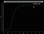
I’ve putted together a test bench to extract the gm, the well-known diode connection with a voltage source varying (Vgs=Vds). I plotted the gm directly by going to the “Results Browser” (because I saved the parameters from the mosfet into a file) and in the same graph I plotted the same gm but now doing the derivative of Id in respect to vgs, that is I’ve done the derivative on the Id vs vgs current.

When comparing both, the results are a bit different:

gm_vs_vgs.png

Anyone is able to tell me why? And which one is more reliable? I would say the gm given by cadence because it might take into account other effects or variables that are out of our range. But I am not sure and I don’t really know.

3rd Question:

With the same circuit mentioned above I’ve plotted the gm/id vs vgs in two ways. The first one was through the file where I saved the parameters from transistor. There we can find a parameter with the name gmoverid. After that what I did was go again to the result browser and ask for the gm and for the id individually and divided one by the other (gm/id). Both plots were plotted against Vgs.

gmOVERid_.png

Now I ask we is that the curves differ? Since the variables were taken from the very same file, but in one I had the result straight away and on the other case I had to compute the value.

4rd Question:

When I try to plot the gm/id without resorting to the “Result browser” from the file that I used to save the mosfet parameters, I get a strange value.

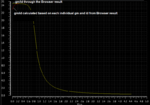
What I did was take the plot from gm where I did the calculation ( deriv of id vs vgs) and divide it by the id vs vgs plot resulting in that strange behaviour that I mentioned: a peak at the beginning of simulation:

gm over id.png

If I start from a different value, like for example 200mV, the curve looks better (obviously). But if we compare it with the above one that I’ve shown, the above one (3rd question) does not have that peak, and it starts from 0.001V.

5th question:

Those curves were taken against VGS and from what I can tell from different sources of either book or papers or slides, people usually plot against VOV. That said, how can I plot the Vov in the x-axis?

Regards.
 

Data taken at different Vds voltage values?
 

Not really. It was in the same conditions. Anyway I got over it :D

I have been playing around and trying to figure out what's the best testbenchs to perform the simulations and other stuffs and I came out with other doubts.

From what I have seen, people who have designed some circuits either in papers, thesis or professors slides, the used Vov or Vgs (IC doesn't count because I am not into it yet). If we analyse some of those documentations we can see that at the end of the day the plots that they used were something like: gm/ds vs gm/id, ft vs gm/id, Id/w vs gm/id or Id/w vs Vgs, Cgd/Cgg vs gm/id, etc. So the Vov or Vgs never comes into picture. Well, with exception of a plot that I have seen Id/W vs Vov.

1st Question:

To plot the Vov (in which I am not sure if it is correct, that's why I am asking), I have mounted a diode connect nmos with a single vdc and swept the Vgs (=vds) then I plotted the Vgs vs Vgs and the Vth vs Vgs (attention that I have used the file to same the ops from the mosfet).

Then I used the calculator to subtract the Vgs from the Vth to get the Vov. Is this correct?

2nd Question:


To plot the gds from the mosfet I have used two voltage source in which the voltage at the gate was Vt+200mV and the other swept the Vds. Then I went to the op and asked for the rout. Is this correct?

3rd Question

What's the best testbench to get the Id/W the capacitor?

4rd Question

The gm/id vs vgs or Vov whatever the x-axis it is, is supposed to by taken with that diode connected mosfet. Then the gm/gds is supposed to be taken with the classic mosfet testbench, each vdc at gate and drain respectively.

Then I can plot without any problem the gm/gds vs gm/ids knowing that each of their x-axis is different???

By the way, there is any rule of thumb to make all this plots regarding the transistor sizes and what voltages to use as VGS and VDS?


I am having some strange curves specially with the gm*rout (if the testbench is correct). I will post later to ask you guys what you think about it.


Thank you in advance!
 
Last edited:

1st Question:

To plot the Vov (in which I am not sure if it is correct, that's why I am asking), I have mounted a diode connect nmos with a single vdc and swept the Vgs (=vds) then I plotted the Vgs vs Vgs and the Vth vs Vgs (attention that I have used the file to same the ops from the mosfet).

Then I used the calculator to subtract the Vgs from the Vth to get the Vov. Is this correct?

Not really. With this procedure you achieve all your above named Id-dependent (ordinate) parameters, indeed, as functions of the independent (abscissa) Vov (that's what you want), however only for the cases Vgs=Vds (that's what you wouldn't want).

Actually it's much simpler: Vov=Vgs-Vth. Plot directly vs. this parameter as x-axis (or simply plot vs. Vgs and shift the ordinate for the Vth value to the right).


2nd Question:

To plot the gds from the mosfet I have used two voltage source in which the voltage at the gate was Vt+200mV and the other swept the Vds. Then I went to the op and asked for the rout. Is this correct?
Yes, but just for the case Vov=200mV

3rd Question

What's the best testbench to get the Id/W the capacitor?
???

4th Question

The gm/id vs vgs or Vov whatever the x-axis it is, is supposed to by taken with that diode connected mosfet. Then the gm/gds is supposed to be taken with the classic mosfet testbench, each vdc at gate and drain respectively.

Then I can plot without any problem the gm/gds vs gm/ids knowing that each of their x-axis is different???

Not at all: you cannot mix or compare cases with Vds=Vgs with cases with Vds≠Vds .

By the way, there is any rule of thumb to make all this plots regarding the transistor sizes and what voltages to use as VGS and VDS?

No; this always depends on your application.
 

Hi erikl thanks for the reply.

I am struggling to get what I want. Bloody plots. I have plotted the basic ones and I tried to make an example and nothing goes as supposed.

1st - gonna try to do this shift thing that you suggested.

2nd - So what's the best way to do it so that I don't be dependent on the Vov = 200mV?

3rd - I meant by Id / W. What's the best testbench to get the Id/W.

UPDATE HERE: I have tried to plot this curve doing the following: diode connected mosfet. Sweep Vgs. Plot Id. Use the calculator to extract dcop variable W and L. Divided W/L. The using the calculator again, Id divided by (W/L).
the same I have applied to get the Id/W. I am following two slides, material, text, whatever. I think that it's in here that I am screwing the thing. Or not. Don't know.

4rd - What I meant was:

To plot the gm/Id I am using the diode connected circuit. So I get the gm/Id vs Vgs.

To get the gm/gds vs Vgs I am using the vt+200mV in the gate and sweeping the Vds.

After this I do the plot gm/gds Vs gm/Id.

This is wrong then?

So in the ECEN 474 homework correction, where they have the plots as solutions, when they are plotting gm/gds this means that they are using the same circuit? They just show the gm/gds vs gm/Id and not in first place gm/gds vs whatever is supposed to be

To finish erikl, I am seen a testbench where they use vds source at the gate and vdc and others as a diode connected. Which one is the best option?

Just for curiosity, in the pictures below, the testbench below the other 2 from the docs I have, the fix the voltage at VDD/2 = 0.9V and they sweep the VGS from 0V to 1.8V.

The diode connected setup both are varied from 0 to 1.8V.

tbs.png

I am trying to do this bloody curves for a 1 week now in my free time. All the free time I had this week was dedicated to this. It's frustrating.

Regards.
 

Hi erikl, thanks for your reply. I've read everything you wrote and I will have to think about it. If I have any question can I come back to you here?

No moving on, I would like to ask other questions about plotting the graphs for the gm/id methodology.


3rd Question:

With the same circuit mentioned above I’ve plotted the gm/id vs vgs in two ways. The first one was through the file where I saved the parameters from transistor. There we can find a parameter with the name gmoverid. After that what I did was go again to the result browser and ask for the gm and for the id individually and divided one by the other (gm/id). Both plots were plotted against Vgs.

View attachment 129254

Now I ask we is that the curves differ? Since the variables were taken from the very same file, but in one I had the result straight away and on the other case I had to compute the value.

Not sure why it differs in your case.
My simulation, the results are exact the same.
 

Status
Not open for further replies.

Part and Inventory Search

Welcome to EDABoard.com

Sponsor

Back
Top