pulkit.vlsi
Junior Member level 1
how can we design a flip flop using latch ?
Follow along with the video below to see how to install our site as a web app on your home screen.
Note: This feature may not be available in some browsers.

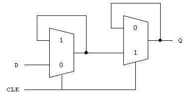
Basic difference between the two is that flip flops are edge sensitive whereas latches are level sensitive. So an edge triggered flip flop can be implemented using Nand latch as following
View attachment 76582
Prashanth.vinnakota,
Can you explain your point? How this will work as latch if the clock is constant, I said this is edge triggered flip flop.
Thanks,
Fpgadsgnr
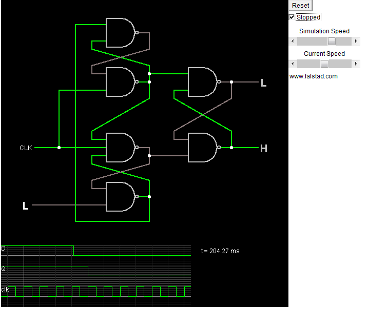
The link below is to an interactive animated simulation of the Edge-Triggered D Flip-Flop shown in post #4.
The website has some more flip-flops (as well as an entire library of circuits).
Click 'OK' when a window comes up asking if you want to load the java applet.
https://www.falstad.com/circuit/e-edgedff.html
A constant '1' signal simply serves as an enable signal for the latch. You will have the input stored when this CLK is constant 1. In fact it is the enable signal for the latch.
Edge triggering concept comes into the picture iff clock is a 0->1->0........ signal. Its better i differentiate the terms by Enable and Clock.
Enable for Latch. Clock for Flipflop.
Hope its clear.
Can you verify your point using the application shared by BradtheRad?
Thanks,
Fpgadsgnr
This will do. Only thing to be remembered is the clock signal must be a pulse input with continuos 1->0->1 transitions. If it is a constant 1 it functions as a latch i.e level sensitive.
Sorry, I wanted you to prove this point of yours, so if you make freq of clock 0MHz then will it become latch? That's absolutely wrong.
Sometimes we use the words flipflop and latch interchangeably. Try to understand this. That doesnot mean that a latch cannot contain a signal called "CLOCK". Remove the clock signal completely and we can surely call it as a latch. Whats the use in having a clock signal operating at 0HZ frequency? Its just a DC signal with Logic '0' or '1'.
Its the type of operation which actually differentiates them. When the output is level sensitive it is latch. Here racing problems will exist.
If the output is changing at clock edges it is exclusively called as a Flipflop.
What you want to explain, it all goes beyond my head. It will be beyond my tolerance limits, if you say that we use words flip flop and latch interchangeably. It's completely wrong when we talk about FPGAs. And by asking you to make CLK freq as 0MHz, I meant to let you do what you had told :
" Originally Posted by Prashanth.vinnakota
This will do. Only thing to be remembered is the clock signal must be a pulse input with continuos 1->0->1 transitions. If it is a constant 1 it functions as a latch i.e level sensitive."
Let's end the issue here, I don't mean to challenge your understanding.
Thanks,
Fpgadsgnr.
What is this? I dint mean to challenge anything. If you can justify that my statements are wrong i will be happy.
In textbook terminology we sometimes mention the word latch inplace of flipflops. But basically as per digital circuits concepts clock doent exist at all in latches.
Do you work on FPGAs? Haven't you noticed the impact of unwanted latches in your design? Now atleast when you are answering to someone's query, you should not be casual and make such statements.
My emphasis was to contradict following of your statement
Originally Posted by Prashanth.vinnakota
This will do. Only thing to be remembered is the clock signal must be a pulse input with continuos 1->0->1 transitions. If it is a constant 1 it functions as a latch i.e level sensitive."
Which stands totally wrong for the circuit, I had suggested, I want to see how you can justify this statement.
Thanks,
Fpgadsgnr
No. I am not an FPGA designer. Is level sensitive operation considered as flipflop? Let me know this.
_Flip-flop_Diagram.svg.png")