Continue to Site

Welcome to EDAboard.com

Welcome to our site! EDAboard.com is an international Electronics Discussion Forum focused on EDA software, circuits, schematics, books, theory, papers, asic, pld, 8051, DSP, Network, RF, Analog Design, PCB, Service Manuals... and a whole lot more! To participate you need to register. Registration is free. Click here to register now.

EM-IR/Current Calculation for a metal wire in layout

Status
Not open for further replies.

Artist27

Newbie
Joined
Sep 5, 2020
Messages
5
Helped
0
Reputation
0
Reaction score
0
Trophy points
1
Activity points
69
How will you calculate width and length of a metal wire if a certain current rating or requirement is given to you?
I know that we can calculate metal width but I am not sure how the metal length comes into play.


Question is about IC, yes?
In old processes length is irrelevant for EM, while for beyond CMOS we are relying on tools (Ansys and Cadence provides relevant tools to get EM/IR on both cell and chip level) and data from foundries (proper rule files for EM).

IR drop is easier to handle as is directly visible in post layout simulation.
 

    Artist27

    Points: 2
    Helpful Answer Positive Rating
The only way length matters is either I*R drop,
or for very short lines there's a limit (forget the
name) below which EM does not happen.

Width, you ought to apply some rule of thumb
(or foundry data, but good luck with that level
of transparency) for over-etch and notching.
Also, at via / contact, effective width is half of
the via circumference / periphery if the via is
self-filled. Tungsten plug systems are different
but I have never had the pleasure of doing a
HiRel part in a tungsten plug via process, to
have dug up the info on that. Another issue to
beware is that the tungsten plug is a resistor
and will locally heat the interconnect attached
to it, jacking your temperature away from what
you might assume (Tj, or Tj plus I^2*R/area*theta_eff).
Temperature is the prime accelerant of failure.

Likewise thickness should be figured at minimum
acceptance film thickness, less any thinning that
may be found at oxide steps or in contact / via
sidewalls.
 

Question is about IC, yes?
In old processes length is irrelevant for EM, while for beyond CMOS we are relying on tools (Ansys and Cadence provides relevant tools to get EM/IR on both cell and chip level) and data from foundries (proper rule files for EM).

IR drop is easier to handle as is directly visible in post layout simulation.

Hi,
Thank you for your response. I worked on FinFET technologies and used Cadence Voltus Fi to get EM-IR on cell level. However, my question is that while doing a simple calculation for metal width using maximum current flow in any metal How does the length of a particular metal comes into play?
Suppose I have a metal length of 5u and a max current rating of 5 mA..how will I calculate the metal width?
In short, how can I calculate width and length of a metal trace using max current rating (given in DRM)?
 

The only way length matters is either I*R drop,
or for very short lines there's a limit (forget the
name) below which EM does not happen.

Width, you ought to apply some rule of thumb
(or foundry data, but good luck with that level
of transparency) for over-etch and notching.
Also, at via / contact, effective width is half of
the via circumference / periphery if the via is
self-filled. Tungsten plug systems are different
but I have never had the pleasure of doing a
HiRel part in a tungsten plug via process, to
have dug up the info on that. Another issue to
beware is that the tungsten plug is a resistor
and will locally heat the interconnect attached
to it, jacking your temperature away from what
you might assume (Tj, or Tj plus I^2*R/area*theta_eff).
Temperature is the prime accelerant of failure.

Likewise thickness should be figured at minimum
acceptance film thickness, less any thinning that
may be found at oxide steps or in contact / via
sidewalls.

Hi,
Thank you for your response. You correctly stated that length matters when we are dealing with IR drop. However my question is that how can I calculate width and length of a metal trace using the maximum current flow rating that is given in the DRM?
 

In FinFET technologies, the current density "rating" (limits) depend on metal line length.

In older technologies, this effect is either ignored, or insignificant - so the length of the metal does not matter, if you want to satisfy the current density (EM) rules - only metal width matters.
 

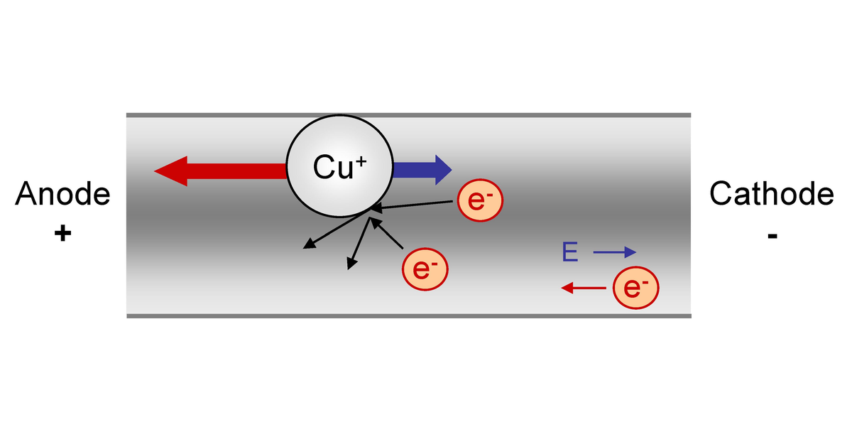
"Blech length" is what I referred to:


If the Blech length is tens of um and you're
in a 12nm flow, that's pretty much infinite
latitude (1000:1) length-wise. You may see
the Blech length reflected in some current-
vs-length rules table as a "breakpoint" in
rule definition / value.

I mostly work in technologies where 10um
won't get you past the device sidewall....
 

if you want to calculate before EMIR run, you can use formula from design manual.
I personally plus 10-30% from max value for margin in calculate.
This kind of calculate is note quite accurate, but it still give enough hint for layout work.

By the way, tools like Custom compiler or Virtuoso (require extra lic) also provides option for checking wire resistance on flight, also not 100% accurate but still better than calculate on spreadsheet :).
 

Status
Not open for further replies.

Part and Inventory Search

Welcome to EDABoard.com

Sponsor

Back
Top