beginner_EDA
Full Member level 4
Hi,
I am using Dual Clock fifo from Altera IP Core and instantiating it as:
The input data width(data) is 4 bit at 250 MHz whereas output(q) data width is 8 bit at 100 MHz.
The continuous input stream is controlled by a trigger signal i.e. if trigger_signal == 1, then only write to fifo otherwise not.
I am struggling to understand how wrfull signal can be coordinate with trigger_signal while setting
wrreq <= 1 ?
Similarly how to coordinate rdempty signal with trigger_signal while setting rdreq <= 1 ?
I tried in this way:
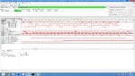
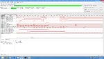
but I end up with some stale data on reading side and first 4 bits on writing side.
In VHDL, I think one can do this using FSM with 3 different processes, 1st process for clocked update of Present state, 2nd for State transition and 3rd for output decode.
but in verilog I am facing problem.
Any idea please?
Regards
I am using Dual Clock fifo from Altera IP Core and instantiating it as:
Code Verilog - [expand]
The input data width(data) is 4 bit at 250 MHz whereas output(q) data width is 8 bit at 100 MHz.
The continuous input stream is controlled by a trigger signal i.e. if trigger_signal == 1, then only write to fifo otherwise not.
I am struggling to understand how wrfull signal can be coordinate with trigger_signal while setting
wrreq <= 1 ?
Similarly how to coordinate rdempty signal with trigger_signal while setting rdreq <= 1 ?
I tried in this way:
Code Verilog - [expand]
but I end up with some stale data on reading side and first 4 bits on writing side.
In VHDL, I think one can do this using FSM with 3 different processes, 1st process for clocked update of Present state, 2nd for State transition and 3rd for output decode.
but in verilog I am facing problem.
Any idea please?
Regards