Continue to Site

Welcome to EDAboard.com

Welcome to our site! EDAboard.com is an international Electronics Discussion Forum focused on EDA software, circuits, schematics, books, theory, papers, asic, pld, 8051, DSP, Network, RF, Analog Design, PCB, Service Manuals... and a whole lot more! To participate you need to register. Registration is free. Click here to register now.

driver compression logic

yefj

Advanced Member level 4
Joined
Sep 12, 2019
Messages
1,192
Helped
1
Reputation
2
Reaction score
3
Trophy points
38
Activity points
7,199
Hello, I have the following circuit where the heart is the BJT.when i put the resistor to be 50Ohms i get a good sine current on the inductor L1 shown below.
But when i put 25 ohms i get compression .
In the compressed version i see that the current going threw the inductor is much higher and it seems like for input voltage of 3.8V the current reaches its maximum and going threw a compression.

does the current compression situation happens because the PNP NPN switch threw other states?
What is the logic of the cause the current threw L1 gets compressed?
Thanks.
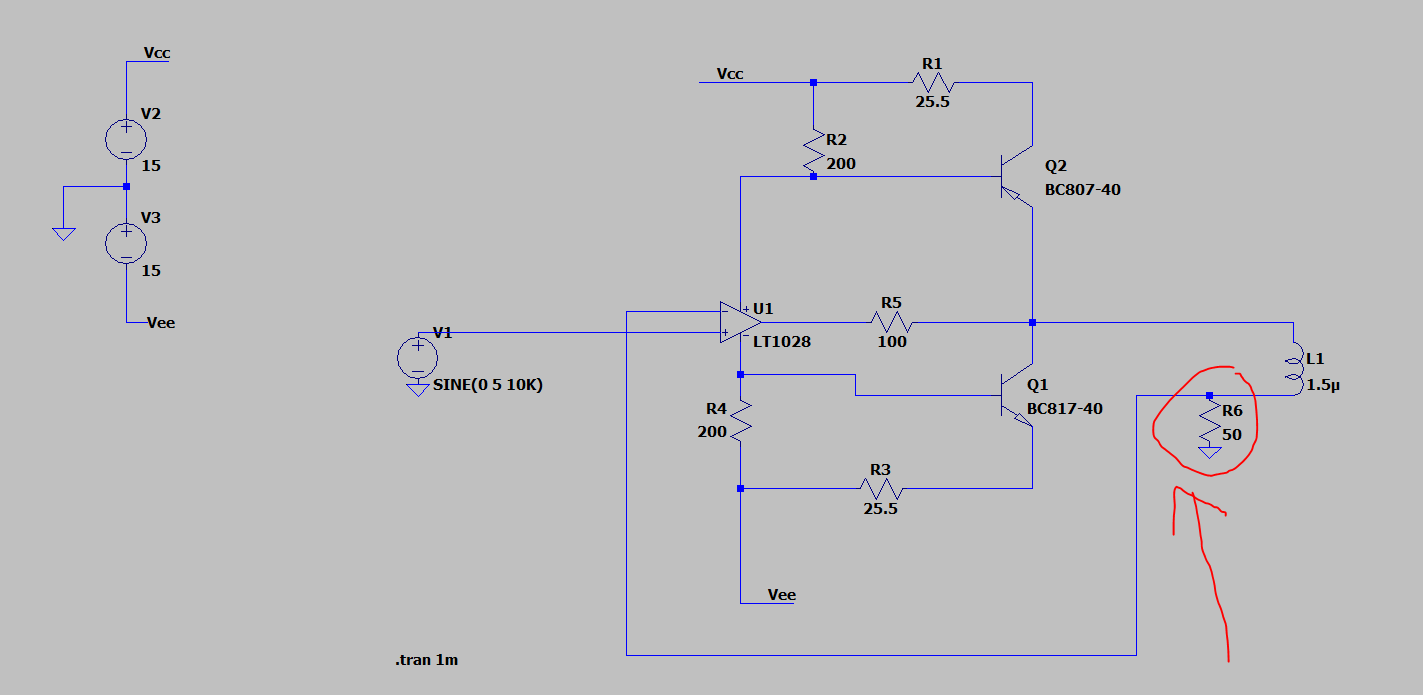
1702656259139.png


1702657019308.png

1702657488455.png
 
Hello FVM,even when i flipped the PNP i got the same compression plot.
hi guess that Q1 and Q2 are not opening simulatiosly.I assume that Q1 and Q2 enter the saturation state at some point Correct?
why saturation state in Q1 and Q2 causes current threw L1 to stop increasing?
Thanks.
1702661195393.png
1702661172191.png
 
Limited voltage swing is a side effect of current boost circuit, no intentional function. It's intended to be used in linear range below compression.
 
its limited current threw inductor swing,thats why i think its probably bjt changes states and cannot supply current no more.
Thanks.
 
Hi,

I´m with Tony.
the external current gain is too low, thus the LT1028 current becomes too high .. and the LT1028 clips.

In a real circuit I guess the tiny BJTs may explode. (did no calculation)

And btw: you have a simulation tool. So use it! Just measure the output current of the OPAMP and compare it with the datasheet limits.

Klaus
 
Hello Klauss,I do see the clipping of current both in the OPAMP and the BJT as shown below.
from data sheet shown bellow the opamp works with 8mA to 11mA.
What is the external current gain of OPAMP?
Is it called by some other name? i cannot see it in the data sheet bellow.
Thanks.


1702668264255.png


1702667865150.png

1702667899626.png
 
It is specified for voltage swing only > 2k. but implied ~ 6mA max

If you wanted 100 mA use an NPN/PNP emitter follower. or maybe a Darlington for more and reduce Vcc, Vee to reduce dissipation < 50% efficient. Use feedback from the emitters.This is similar to Class B audio but with excess GBW error is small.

1702668989942.png
 
Last edited:
Hi,

I´m a bit stressed today. So please first things first.
I asked you to measure the OPAMP output current.
Please do so and show us the chart.

Klaus

added:
Is it the red channel of the shown chart?
--- Updated ---

I guess it is.
It makes sense, it shows a clip at about +/-22mA.

Now you refer to the OPAMP supply current. It is the current (often referredas quiescent current) that internally flows from V+ to V-.
Positive output current gets added to the V+ current.
Negative output current gets added to the V- current.

So if you have 9mA quiescent current and 22mA output current, then
The current at V+ is 9mA +22mA = 31mA
The current at V- is just 9mA.
(mind that this is a raw view, for a more detailed view one needs to know all the internal circuits, gain.. and so on)

Now I talked about "external current gain". This is not an LT1028 internal thing at all. (thus external) it´s the gain of the bjt circuit.
The (differential) DC gain is dominated by R2 and R1. It´s about R2/R1 = 200/25.5 = 7.8
This means if V+ current changes by 1mA the load current by 7.8mA (collector current) + 1mA (LT1028 output current).

Now it´s your turn.
What is your expected load current range?

Klaus
 
Last edited:
I basically don't understand the discussion.

The shown current booster is working well and provides output current up to the designed limits. If you don't understand immediately why output swing is limited with given component values, look closer on the simulation results.
Particularly plot Vce of both transistors together with output voltage.

I believe in learning circuit design by analyzing circuits yourself.
 
It is difficult to predict the balance of quiescent collector currents in this design and being current sources with high impedance offers few advantages outside the Op Amp.

Negative feedback will lower the 100 ohm output impedance but load regulation will still be poor. As a result asymmetrical voltage saturation occurs.
 
Hi,

The 100 Ohms output is to provide current to the load, especially at low load currents, when the "booster" via the BJTs is not active yet.
This helps to reduce the classical CLASS B distortion.

I agree with FvM that the original circuit was properly designed.
Increasing the current needs more than just modifying one resistor. The whole circuit needs to be adjusted.

The circuit is not new. I´ve seen similar circuits decades ago to drive headphones with audio quality. With the "constant" current output they tried to immitate tube sound.
I never was convinced about the concept.

Klaus
 
Hello Klauss, i was able to reduce the current saturation by playing with R1 R2 pairs of the circuit bellow.
Also i was able to reduce the total current on the inductor by playing with R5.
You said that according to the datasheet my opamp could burn under some current condtions.
the quicent current of the opamp is 8mA the output is 22mA .
Where is the data sheet bellow says that it could burn?
Thanks.


1702710615819.png


1702710942279.png
 
Hi,
Also i was able to reduce the total current on the inductor by playing with R5.
I´m confused. You first rduced the value of R5. Usually one doe this - since it´s the shunt for current measurement - to increase the load current.
Now you said you reduce the load current, so you made the value of R5 a bit higher, I guess. So somem kind back in direction to the previous value.

Now my basic question: You modified the circuit. Why?


You said that according to the datasheet my opamp could burn under some current condtions.
the quicent current of the opamp is 8mA the output is 22mA .
Where is the data sheet bellow says that it could burn?
Again I´m confused. Are you referring to this?
In a real circuit I guess the tiny BJTs may explode. (did no calculation)

Klaus
 
Now my basic question: You modified the circuit. Why?
Problem is that no design goals have been yet specified. As stated the circuit works with original dimensioning, except for unsuitable BJT transistors which are loaded with a multiple of their rated power, as already mentioned. That's no problem in simulation but a real circuit must use transistors with sufficient power rating, otherwise it may "explode".

Increasing the current needs more than just modifying one resistor. The whole circuit needs to be adjusted.
You name it. There are complex interdependcies. It should be also mentioned that current amplifier phase margin with inductive load is rather low. A small change makes it oscillating.

All in all, KlausST's reservations against this specific amplifier topology are well substantiated. On the one hand it's an elegant way to setup a class AB output stage with low component count and good performance. On the other hand, its behaviour is complex and tuning far from being easy.
--- Updated ---

I guessed in post #11 clipping with modified R6 would be mainly caused by BJT saturation. That's wrong. We see essentially OP current limit, translated by R2/R1 respectively R4/R3 resistor ratio in output current limit.
 
Last edited:
Hello,from the data sheet bellow the BJT can handle 500mA ,as you can see the simulation Ic of the BJT below is only 150.
Its very important for me to understand Klaus words shown below.
Its seems like i am missing a point where the Simulation current exceeds what the OPAMP was designed to.
Where can i see it in the data sheet?

"
the external current gain is too low, thus the LT1028 current becomes too high .. and the LT1028 clips.

In a real circuit I guess the tiny BJTs may explode. (did no calculation)

And btw: you have a simulation tool. So use it! Just measure the output current of the OPAMP and compare it with the datasheet limits.

Klaus"


1702724998235.png

--- Updated ---

UPDATE:
Hello , i have attached the ASC in RAR file file of my simulation.I want to test the states of the PNP based on the data sheet.
In the end you can see the PNP current Vcb Vce Veb.
near clipping
Veb=660mV
Vce=-15V
Is it a realistic state?
What state is it?

Thanks.
https://www.alldatasheet.com/datasheet-pdf/pdf/16110/PHILIPS/BC807-40.html
1702729188097.png
1702729159236.png
 

Attachments

  • driver.rar
    807 bytes · Views: 40
Last edited:
Hi,

when I said it explodes, it means it is overheating until self destruction.

Heat is not caused by current, it is caused by power. And power is V x I.
And there is a power rating for the BJT. Look at the datasheet.
This power rating depends on heat spreading, thus PCB copper area, soldering, pin length, air flow .. and so on has influence.

Klaus
 
Using thermal resistance from junction to ambient Rja, you multiply by power to get the junction temperature rise above ambient. Even if it works with reduced lifespan at 125'C junction or a 100'C rise above 25'C , you would never design it for this and instead use a conservative 60'C rise above 20'C or a 40'C rise above 40'C ambient to maximize reliability and reduce the risk of burning your finger and heating up components nearby that are temperature sensitive.

You NEVER design to meet the ABSOLUTE MAXIMUM SPECS, you design to always have margin which offers a more favorable lifespan.

For example you would never design a product to use capacitors that only last 1000 hrs. Yet this is how they accelerate lifespan to meet a minimum of 1000 hrs by raising the temperature of testing to one of several grades. 85'C, 105, 115. This is due to the fact that Arrhenius Law of chemistry predicts that all components will have a logarithmic failure rate where lifespan reduces 50% for approximately every 10'C rise in junction temperature above ambient. This has been proven and is used to compute reliability of products, separately from manufacturing defects.

This is why e-Caps are rated for 1kr hour reliability due to Arrhenius Law and the fact that dielectric interfaces suffer from more stress than resistors or semiconductors.
--- Updated ---

For example the SC-70 case transistor has an Rja = 272 'C/W so at (Ic=200 mA) * (Vce=5) = 1W pk and with a sine clipped will be about 50% average power of 0.5W or 131'C above your worst case ambient . So you would need a much bigger part rated for perhaps 10W with at least 5x5cm of Cu-clad PCB heatsink to operate it normally or a 5W part with an external heatsink to run cool and not heat up your electrolytic capacitors nearby.

- this is a "poorman's analog power amp" and there are much better solutions.
--- Updated ---

For example the SC-70 case transistor has an Rja = 272 'C/W so at (Ic=200 mA) * (Vce=5) = 1W pk then the opposite polarity 60 mA*19V~1.1w. Fried eggs anyone?

So you would need a much bigger part rated for perhaps 10W with a Cu heatsink to operate it normally or a 5W part with a small heatsink.
 
Last edited:
This design is a 30W analog audio power amp. Note how the internal structure looks like an Op Amp except it is discrete for better low impedance output and external compensation with C3 and gain control by (C9+R9)/R8 ratio.

The driver stage with power Darlington's use emitter current sense resistors of 0.4 Ohms drawing only 20 mA quiescent current but can drive a 1.5 A load with a CPU sized heatsink. The 0.4 Ohms was chosen for a TIP Darlington power device and limit current to about 0.7V/0.4 ohms = 1.75A which would exceed 30W if the output was short circuited to ground while clipping, but survive with a good heatsink.


1702743337753.png


This is still not enough current to drive an 8 ohm subwoofer but shows good balance and active current limiting.


In your old design, you would need to know the internal OA current limit and use a ratio with the Rb,Re and 100 ohm load to compute the transistor current limit to stay within conservative thermal design limits of say 80'C for junction temperature at maximum ambient.
 
Last edited:

LaTeX Commands Quick-Menu:

Similar threads

Part and Inventory Search

Welcome to EDABoard.com

Sponsor

Back
Top