Continue to Site

Welcome to EDAboard.com

Welcome to our site! EDAboard.com is an international Electronics Discussion Forum focused on EDA software, circuits, schematics, books, theory, papers, asic, pld, 8051, DSP, Network, RF, Analog Design, PCB, Service Manuals... and a whole lot more! To participate you need to register. Registration is free. Click here to register now.

DRC Violations. Please Help. Urgent.

sincplicity

Newbie level 4
Joined
Apr 3, 2023
Messages
7
Helped
0
Reputation
0
Reaction score
0
Trophy points
1
Activity points
43
I am urgently trying to resolve some drc errors for a tsmcN65 process.

The errors are related to enclosure such as DM1.EN.1 with rule defined as:

DM1.EN.1 { @ Enclosure by chip edge >= 2.51 um
DUM1 NOT (SIZE CHIP_CHAMFERED BY -DM1_EN_1)
}

The area is defined by Pr Boundary layer. The defined edge to a violation shows >= 2.5 um distance? What am I missing?

I have requested a DRM but have not received yet. Thanks in advance!
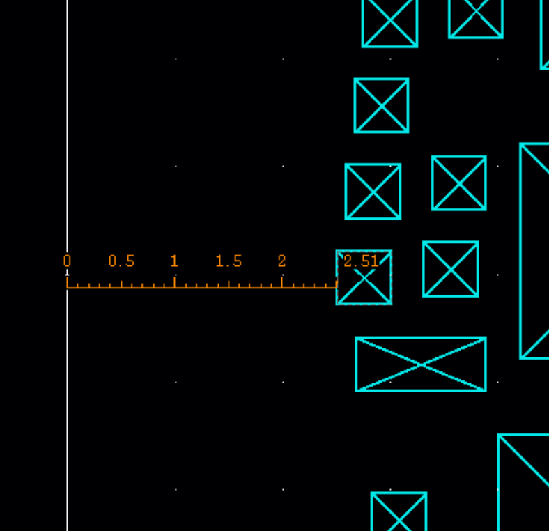
1714770678234.png
 
Drill into the DRC deck and see what defines "chip edge".
It may not be prBoundary. Might be "bulk" or "scribe" or
something like that.

First step to debugging is understanding what the rule
is supposed to be telling you. Do not assume developer
clarity or communications skills, flowed all the way to the
error report line nor that you're imagining their meaning
as meant.
 
Thank you for the fast reply. I pulled up the DRC deck and am looking through it.

Are those key words to look for?
--- Updated ---

I found these lines within DRC that are used to define the chip, I believe. ChipWindowUsed is not currently defined.

There is list of EXTENT layers that get mapped to the MT_LAYERS but do not know which extent layer to used. They seem to be defined from physical layers.

#IFDEF ChipWindowUsed
LAYER ChipWindow 500 // layer number for constructing chip boundary
POLYGON xLB yLB xRT yRT ChipWindow
CHIP = PUSH ChipWindow
#ELSE
CHIP = EXTENT MT_LAYERS
//CHIP = EXTENT
//CHIP = EXTENT CELL "*" ORIGINAL
#ENDIF
 
Last edited:
I start with searching the error text, to find the rule code; then follow the logic backwards through the deck until you can identify the layer precursors that make the logical args.
 
looks like metal fill was applied before chip was assembled and violated some rules? hard to say, the screenshot is not informative
 

LaTeX Commands Quick-Menu:

Part and Inventory Search

Welcome to EDABoard.com

Sponsor

Back
Top