Continue to Site

Welcome to EDAboard.com

Welcome to our site! EDAboard.com is an international Electronics Discussion Forum focused on EDA software, circuits, schematics, books, theory, papers, asic, pld, 8051, DSP, Network, RF, Analog Design, PCB, Service Manuals... and a whole lot more! To participate you need to register. Registration is free. Click here to register now.

drc error

omar97

Newbie
Joined
Apr 1, 2024
Messages
5
Helped
0
Reputation
0
Reaction score
0
Trophy points
1
Activity points
33
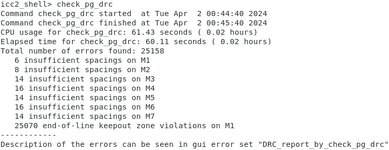
I face a problem, during powerplanning when I connect power and ground nets to power and ground pins, then when I check pg drc, I get a huge number of drc violations in metal 1 between vdd and vss metals.
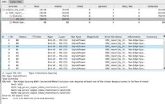
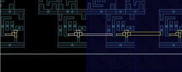
The drc error is end of line keepout zone violations on metal1 inside standard cell.
I can't understand this error and I don't know how to solve it.
So please help me to understand why I face this error?

I use technology TSMC 65nm
 
Last edited by a moderator:
Hey there! It sounds like you're dealing with a tricky issue in your power planning process. The end-of-line keepout zone violations on metal1 inside standard cells can be quite frustrating to deal with, but don't worry, we can work through this.

Firstly, let's break down what might be causing these violations. Typically, end-of-line violations occur when there's insufficient space between different metal layers, leading to potential shorts or other manufacturing issues. In your case, it seems to be happening specifically between VDD and VSS metals, which are your power and ground nets, respectively.

One common reason for this could be improper spacing or routing of your power and ground nets. Check if there's any overlap or crossing between VDD and VSS metals, especially within the standard cells. Sometimes, even minor misalignments can lead to these violations.

Additionally, ensure that your standard cell libraries are properly set up with the correct design rules. Sometimes, discrepancies in the library settings can cause unexpected DRC violations.

Another thing to consider is the width and spacing of your metal1 traces. If they're too close together or too narrow, it could trigger DRC violations. Double-check your design rules to make sure you're meeting the minimum requirements for metal1 spacing.

[REMOVED NON ENGLISH REDIRECT LINK]

Hang in there, tackling DRC violations is definitely a part of the learning process in chip design. Keep investigating and tweaking your design, and you'll get through this hurdle. Good luck
Thank you sir, and I will read surah Al waqiah ❤️ ISA.
But one thing to take into account I see in layout gui that the spacing actually is very large between Vdd and Vss.
Also I see one neighbour standard cell don't get this violation.
So, I am not sure is that actually a problem?
And also before connecting power pins an power nets there is 0 drc error.
I don't make power network complex.
But after running command: connect_pg_net
 
Post a screenshot if you can (make sure not to show tech-specific details)
Is the issue all over the die or only on corners or on specific rows?

Where are you checking the violations? Innovus will give you a lot of false positives, you should not rely on that. Calibre is the way to go. And LVS.
 
Post a screenshot if you can (make sure not to show tech-specific details)
Is the issue all over the die or only on corners or on specific rows?

Where are you checking the violations? Innovus will give you a lot of false positives, you should not rely on that. Calibre is the way to go. And LVS.
Hello sir,
These are screenshots of my errors.
 

Attachments

  • IMG-20240402-WA0001.jpg
    IMG-20240402-WA0001.jpg
    60.7 KB · Views: 37
  • IMG-20240402-WA0002.jpg
    IMG-20240402-WA0002.jpg
    143.1 KB · Views: 40
  • IMG-20240402-WA0000.jpg
    IMG-20240402-WA0000.jpg
    195.5 KB · Views: 37
These are inside the std cells, this should not happen. A few ideas:
- you are using cells from the wrong tech/flavor
- your errors are false positives and you should check with calibre
- your design is missing std cell rails. this might affect the errors you are reporting, it might not.
 
For some reason line-end via enclosure seems to get special
treatment in more modern PDKs. And if cell layouts come from
a different foundry source / version / vintage that rule may vary
or may not have even been a consideration.

That rule should flag even on the lowest level cell containing
such a feature. OP mentions it only after higher level construction.
It's possible that the rules apply differently to power nets than
signal-only, and then there could be marker layers to steer that
away from intra-std-cell features (if placed, and if deck cares to
look).

Definitely check for DRC of same type on a lonely cell top level,
to check out these possibilities and, if you find the errors in the
primitive cells, go back to the foundry (after checking that the
PDK instructions don't actually cover these subtleties) for some
advice on why their cells show busted and what to do to get past
tape-in checks (which may well be Caliber and other tools just
spray errors, because not-Caliber, and PDK developers do not
care about tools they don't have to support, already having
swallowed the Caliber license).
 

LaTeX Commands Quick-Menu:

Part and Inventory Search

Welcome to EDABoard.com

Sponsor

Back
Top