Continue to Site

Welcome to EDAboard.com

Welcome to our site! EDAboard.com is an international Electronics Discussion Forum focused on EDA software, circuits, schematics, books, theory, papers, asic, pld, 8051, DSP, Network, RF, Analog Design, PCB, Service Manuals... and a whole lot more! To participate you need to register. Registration is free. Click here to register now.

dispute about a Simple Mosfet logic circuit

Status
Not open for further replies.

pelvisp

Newbie level 5
Joined
Oct 29, 2009
Messages
10
Helped
1
Reputation
2
Reaction score
1
Trophy points
1,283
Location
israel
Activity points
1,400
Hello all,

I hope this is the right place to ask this kind of simple question:

I would appreciate ur opinion on this mosfet logic circuit function.
I have a dispute with a friend...

I say the function is vout=[A'BCD'+ABC']' and he sais: vout=[A'BCD'+A(BC)']'

anyone?

tx in advance,
pELVISp.
 

Attachments

  • logic.jpg
    logic.jpg
    251.5 KB · Views: 164
Last edited:

First you should correct the circuit. The state of Q3 and Q5 ist partly undefined because of missing loads. At present, the output will be none of the claimed functions.
 

isnt Q4 acting as an active load for the entire PDN?
 

isnt Q4 acting as an active load for the entire PDN?
If you don't expect the current source by Q4 to flow through the gates of Q3 and Q5, it hardly can.
 

Perhaps some assumptions are needed , ideal transistors , loadings and current driving matters. nevertheless , the circuit should have a logic output.
my thoughts lead me to the answer vout=[A'BCD'+ABC']' , I'll explain:
I looked for the input signals that would make the PDN (Pull Down Network) active , meaning grounding Vout.
there are two paths for this:
1) Q3 on and D input as ground. for Q3 to be on Q1 and Q2 must be on while C is "High". leading to A'(Q1on)B(Q2on)C( Q3on)D(ShortVouttoGround) = A'BCD'
2)Q5on and Q6 on, for Q5 to be on you need Q2 to be on and C "low".leading to B(Q2on)C'(Q5on)A(Q6on)=BC'A

so finally: Vout'=A'BCD'+BC'A => Vout=(A'BCD'+BC'A)'

Is there anything fundamentally wrong with my analysis?
again, I would appreciate any input
Tx.

P.S
I apologize for multiposting , I wasnt sure where this post would be best placed , here or Electronic Elementary Questions forum
 

The output is not defined when A(B' + BCD') is true.

Hehe, I had to edit this post a few times before I got it right...
 
Last edited:

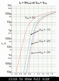
Reading pelvisp explanation, I think the fault is in assuming, that a transistor would be turned on with zero Vgs and negative Vbs. But this isn't the case with usual transistors.

I suggest to sketch a truth table containing the states on, off or X for all transistors. You'll see, that the output is only defined for 7 input combinations.
Out = 0 for ABC' = 1 (2 cases)
Out = 1 for A'BC' + A'D = 1 (5 cases)
Out = X for the remaining 9 cases

P.S.: I see, that I wrongly assumed Q3 could be turned on. So one more X case
Out = 1 for A'D = 1 (4 cases)
 
Last edited:

It is easy to get confused by this problem!

My previous posting was wrong:cry:

I have now checked again, and I get:

Out = 0 for A'BCD' + ABC' (3 cases)
Out = 1 for A'D + A'BC'D' + ABCD (6 cases)
Out = X for A'B'D' + AB' + ABCD' (7 cases)
 

The result depends on assumed transistor properties. In your recent result
Out = 0 for A'BCD' + ABC' (3 cases)
the term A'BCD' assumes, that Q2 can turn on with B = C = 1

Looking at a typical NMOS characteristic, it can never turn on with Vgs = 0


P.S.: A'BCD' will actually turn Q2 partly on. If Vgs,thr is sufficient low, Q3 can pull Vout low. But in ABC', Q5 won't fully turn on. So it depends on your level definition, if you accept it as a Vout = 0 case.
 
Last edited:
I agree completely with the previous posting.

The title of this thread is misleading, the circuit is not "simple" and it is also not completely "logic" (digital). For some input combinations it is a linear circuit,
and for other combinations floating gates make the output unpredictable.
 
well....

after discussing this question with my lecturer i was glad to find out i was right about my answer Vout=[A'BCD' + ABC']' . btw this was a question from a midterm exam in digital electronics for a electrical engineering degree...

but after reading your posts, im starting to second guess what i thought i understood. I repeat my analysis in short:

to find paths that would ground Vout and thus finding Vout=0 and the other combinations which dont ground vout , tie vout to Vdd by the (always) on Q4 and thus finding Vout=1...
(also note that Q1 and Q2 are bidirectional - Source and Drain terminals can swap roles to find Vgs)


So now, im more concerned about these floating gates , partially on\off Qs , loadings and current driving matters !
Any suggestions on a software to run this curcuit and find out how appliciable/severe the assumptions needed to solve this as my lecturer did?I guess I can use orcad pspice, but i have a feeling there is a simpler way...
(my first guess , is that there will be some need to play around with the transistor sizing to get the right current driving)

again, ur responses and insight were and are much appreciated.
 
Last edited:

This circuit is not as simple as your boolean equation because the previous state would affect the output.
For example, you have B=1, and C=0, which forces Q5 on(assuming pull-up keeps charging the Vout node), and then B becomes 0,which makes Q5 driven by a floating node which MAY keep Q5 on. This means the boolean equation would be Vout = ~A, regardless of other inputs' level, for some time until Q5 get shut down when Vout level drops.


You need to run circuit simulators such as spice to verify this, but you probably need to specify the initial condition to make the circuit work in a deterministic way. No other way because the threshold voltage would play as well.
 
Last edited:

after discussing this question with my lecturer i was glad to find out i was right about my answer Vout=[A'BCD' + ABC']' .
The statement seems somewhat ignorant considering the previous posts. The answer may be correct under several prerequisites, that haven't been said, e.g. transistor threshold voltages, supply, output level considered as logical '0'. Without these definitions, the "digital" circuit behavior is partly undefined, and it's correct to mark the respective states as 'X'.

P.S.: Finally, your claimed solution can't be correct, even under optimistic assumptions for the transistor parameters.

With the input vector "0000", Q2 will be surely turned off. Thus the gate of Q3 is floating, Q3 may be either on or off (depending on a previous input state). Q6 is surely turned off, but because of the unknown Q3 state, Vout is also unknown.
=> Vout=[A'BCD' + ABC']' does not describe the circuit behaviour correctly, as said before.
 
Last edited:

Status
Not open for further replies.

Part and Inventory Search

Welcome to EDABoard.com

Sponsor

Back
Top