Continue to Site

Welcome to EDAboard.com

Welcome to our site! EDAboard.com is an international Electronics Discussion Forum focused on EDA software, circuits, schematics, books, theory, papers, asic, pld, 8051, DSP, Network, RF, Analog Design, PCB, Service Manuals... and a whole lot more! To participate you need to register. Registration is free. Click here to register now.

Diplexer design - combining BPFs

Status
Not open for further replies.

borgmater

Newbie level 4
Joined
Jun 19, 2016
Messages
5
Helped
0
Reputation
0
Reaction score
0
Trophy points
1
Activity points
41
Hello everyone ! Im kinda new to this forum, but ive been watching posts for some time and i think the information here are amazing :) So i thought i give it a go.

Im designing a diplexer within frequencies 2500-2570 and 2620-2690 MHz with band pass filters in microstrip technology, Agilent ADS 2015.01. I have designed BPFs separately, but i dont know how to join them in the simplest way possible, without using additional components ? Any advance is appreciated :)
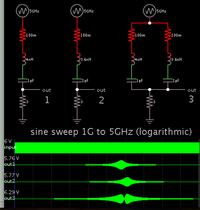
 

A series LC makes a narrow bandpass filter. Add a second LC in parallel. Then you have dual center frequencies.


It illustrates one method although it isn't necessarily the best method. Your project may require a different concept.
 

i meant something like T-junction or Y-junction, a power divider of some sort, but im not sure how to calculate it. btw, there are lumped elements, im talking about microstrip :)
 

I have designed BPFs separately, but i dont know how to join them in the simplest way possible
You'll connect them in parallel and adjust the filter input elements for the additional load. In other words, you can't design them actually separately.
 

Yes ! Maybe i expressed myself in a clumsy way, but thats what i actually want, but dont know how to do. If i wanted everything to match 50 Ohm, how is that achievable ? How long and wide should my input feed line be ? And how to calculate each feed line for each filter ?
 

The answer is that both filters must be designed in aware of the other elements and connecting transmission lines. My approach would be to make the interconnect as short as possible and optimize all filter elements iteratively to achieve the defined overall diplexer characteristic.

May be you find a more systematical approach in literature.
 

I could not agree with you more, thats an excellent advice, but dont get me wrong, i knew that already :) Could you maybe point me to the right literature where i could find formulas or example calculations ?

In short, i have 3 ports, port 1 is where the signal comes from, and ports 2 and 3 are the lines for different frequencies. When a freq2 signal comes from the port 1, it needs to go to port 2 and be invisible for port 3, and vice versa for freq3 signal. In order to do that, i need calculations for input lines of both port 2 and 3.
 

The point is that off-band filter isn't invisible. In case of an ideal band pass, |s11| = 1, anywhere at the unit circle. This input impedance is transformed by the interconnect line (s11 rotated). So one option would be to adjust the line length to get s11 = +1 at the T junction. In this case, the filter would be actually "invisible".

A real filter will show a certain |s21| amount in stop band and s11 moved a bit towards the origin.
 

Status
Not open for further replies.

Part and Inventory Search

Welcome to EDABoard.com

Sponsor

Back
Top