Continue to Site

Welcome to EDAboard.com

Welcome to our site! EDAboard.com is an international Electronics Discussion Forum focused on EDA software, circuits, schematics, books, theory, papers, asic, pld, 8051, DSP, Network, RF, Analog Design, PCB, Service Manuals... and a whole lot more! To participate you need to register. Registration is free. Click here to register now.

Diodes extraction problem with Calibre Interactive LVS

Status
Not open for further replies.

Narcisuss the Reborn

Newbie level 4
Joined
Mar 23, 2022
Messages
7
Helped
0
Reputation
0
Reaction score
0
Trophy points
1
Activity points
100
Hello!

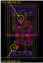
I have a problem with LVS checking of my design with Calibre Interactive. I am sure that the problem is that Calibre (I use 2021.1 version) do not extract diodes (N+ / P-Sub and P+ / N-Well) from the layout by default. So LVS (Comparison Results) reports about Discrepancies - Incorrect Instances (** missing instance **). If I cut off diodes in netlist there are not any LVS errors.
Moreover there are 66 diodes in my circuit but there are only 23 messages about missing diodes.
Notably that it is Calibre problem rather than design because I checked the very cell and have been reported by the same errors.
I also think this is Calibre setup feature because I’ve read that there is Extract Diodes option in the other Calibre versions in Customization Settings menu. But there is not such menu in my version at all!

Could someone to help me with setting up Calibre to correctly extract diodes from layout?
 

I work in kits which embed diode instances under the MOSFETs
so that everything that might be extracted, has its mate. I'd
expect that a lot (maybe all) of the discrepant diodes are
NWell-psub wells, which another foundry requires the designer
to manually place and set geometry properties of dnwell for
every distinct NWell region.

Are you convinced that the discrepant diodes are indeed the
N+/psub and P+/Nw, MOSFET S/D junctions and not those
"not a device" Nw/Psub (unless you look close, or bias wrong,
or are making a bandgap with substrate PNPs) features? Or,
does "no diodes" setting just happen to kill the Nw/Psub
diode errors as well?
 

Thank you for your answer!

As an example I attach schematic and layout of AND cell with aforementioned diodes (they are for ESD protection as I suppose). These diodes have their own recognition layer in layout view. It seems that Calibre doesn’t recognize this layer that’s why it reports about missing devices in layout (gds). But as I said it reports about absence of only part of the total number of diodes (maybe this relates with Calibre specific).
When I said that have cut off diodes I meant that I’ve commented them in netlist file so Calibre LVS can’t read them.
 

Attachments

  • AN2LL_layout.png
    AN2LL_layout.png
    610.8 KB · Views: 168
  • AN2LL_schematic.png
    AN2LL_schematic.png
    15.8 KB · Views: 173

OK. My hot take is, those circled "diodes" are antenna diodes
baked into the standard cell layout. The recognition layer may
be to help antenna rule checks or may be to apply "special
rules" to what may be a "sub-minimum", special purpose device.

However, to my eye these diodes lack "active" and "contact"
and counter-dope layers (P+ in Nw or N+ in Pw). Maybe those
last are turned off, or Booleaned off the active*well_type, or
are line-on-line "keyholed" such that I can't make it out (I
always, always make my own private layer table with N, P
features' fill stipple and color set up so I can see them plainly -
since I'm an old bipolar analog guy and stacked juctions is
how we roll).

If those features are missing then those diodes would be
malformed and righteously unrecognized. However, I'd
hope that a well constructed extract / drc rules combo would
somehow light up "unrecognized" features for this kind of
reason.
 

These antenna diodes have active layer (maybe can’t be seen) but they lack of contact layer indeed. The tungsten local interconnect layer (LIL) is used instead it (you can see connection from source regions of transistors are made with this LIL layer too without contacts on MOS side, orange color). I’ve even tried to add contacts for diode but without effect. P+ and N+ layers are also turned on (pink and yellow colors on the picture respectively).

I still think that’s Calibre extraction problem because there is no errors during stream out of the gds file - all layers are read out correctly.

Thank you for your help anyway!
 

Status
Not open for further replies.

Part and Inventory Search

Welcome to EDABoard.com

Sponsor

Back
Top