Continue to Site

Welcome to EDAboard.com

Welcome to our site! EDAboard.com is an international Electronics Discussion Forum focused on EDA software, circuits, schematics, books, theory, papers, asic, pld, 8051, DSP, Network, RF, Analog Design, PCB, Service Manuals... and a whole lot more! To participate you need to register. Registration is free. Click here to register now.

Diode forward voltage drop at lower forward current

vaibhavwaman

Newbie level 4
Joined
Dec 26, 2009
Messages
7
Helped
0
Reputation
0
Reaction score
0
Trophy points
1,281
Location
mumbai
Activity points
1,370
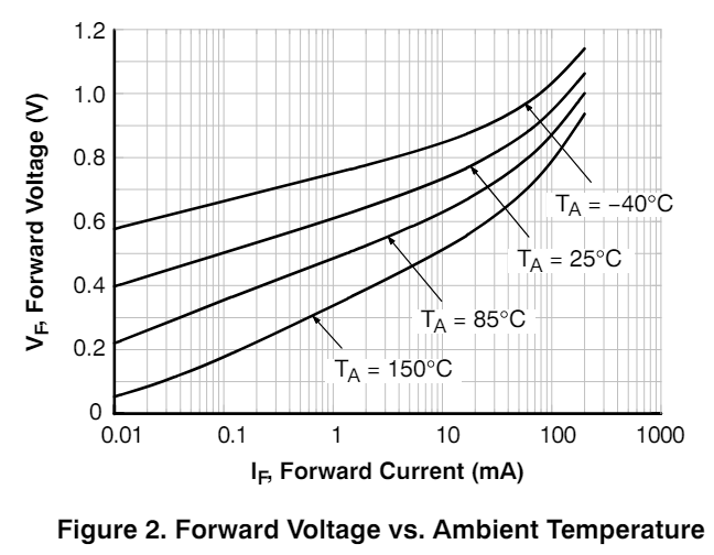
Is making linear approximation for calculating forward voltage drop at lower current than 10uA is good option ? I want to pass current approximately 100nA via this diode and want to understand forward voltage drop in this case ? Or is their any specific reason for which datasheet dont give forward voltage value for very low forward current ?
1713278806015.png
 
That graph is logarithmic on x axis, so no on a linear approximation. You
could use power curve fit or least squares to do it. Keep in mind thats a
"typical" curve, not worst case.

If you are measuring T with it one could use a cal routine to aid in improving
accuracy....

The dual current single diode method, attached.


Regards, Dana.
 

Attachments

  • 001-60590_AN60590_PSoC_3_PSoC_4_and_PSoC_5LP_Temperature_Measurement_with_a_Diode.pdf
    1.5 MB · Views: 29
I want to pass current approximately 100nA via this diode and want to understand forward voltage drop in this case ?
As noted the drop is logarithmic with current.
At 25°C the drop shown is about 0.2V for a two order of magnitude drop in current, so the drop from .01mA (10µA) to 100nA should also be about 0.2V, giving a forward voltage of about 0.2V at that current.

Below is the LTspice sim of a similar diode curve showing slightly over 200mV drop at 100nA:
(Note I had to do the sim at 15°C to reasonably match the 25°C curve of the graph you posted.)

1713282590118.png

is their any specific reason for which datasheet dont give forward voltage value for very low forward current ?
No, it's just that most applications don't operate at that low current, so they don't post it.
 
Last edited:
Not all diodes are the same for leakage due to the geometry and passivation of the Si dielectric barrier surface encapsulation, which is < 1um thick.
All diodes are thermal sensors with voltage when forward biased (NTC) and current sources with leakage current when <= 0V. Above 300 'C this leakage power poses a threat due to the much higher heat density and higher thermal resistance, (if applied with reverse voltage)

ref: https://www.researchgate.net/public..._surface_leakage_reverse_current/figures?lo=1

Here is a low leakage Si diode.
Plastic SMD package
• Low leakage current: typ. 3 pA @ 25'C

If you need leakage current to be constant, make an SMD oven above room temp with a thermistor, regulator,10 mW SMD resistor all attached to the diode with styrafoam insulation. I've done this to make a cheap XTAL OSC. into an OCXO.
1713287572402.png


Keep in mind if forward biased, 200 mV/100 nA = 2 Gohms equiv

I suspect the Space Charge Limited (SCL) model of this Poole-Frenkel (PF) effect advanced by (heavens to) Murgatroid and Boole are such that my hunch is the equivalent circuit is constant RC varicap. The Voltage-controlled capacitance or Varicap effect is found in all diodes created by the reverse bias E-field effect to makes the leakage resistance and C constant at a fixed Temp. Tau=VR/IR * C might be temporarily constant while reverse leakage increases and capacitance reduces with increasing reverse voltage until the temperature changes.

But you might find the answer in this thesis. (TL;DR)

The plastic SMD chip is black to block light which is another source of leakage current from the photo-electric effect in all diodes, transistors and IC's.
 
Last edited:
The logV/I characteristic breaks away from the ideal log-linear
at both high current (Rs) and low current (loss of ideality from
recombination / defectivity). Recombination can be
"modulated" post-fabrication by electrical or radiation abuse.

These latter are "high scatter" lot to lot, wafer to wafer, die to die
and go/no-go leakage @ Vr is about the best you can expect
(if devices are even probed / sorted at all).

Layout nonuniformities (like the corners of an ortho layout) can
in effect create a "two tiered justice system" where the corners
conduct early and the flat edges later and the bottom plate later
still, adding inflection-points to the I-V curve even up where
you'd expect log-linearity (think about superimposing 3 diodes
of grossly different size and doping, in parallel).

In my curve-pulling I see this below 100-200mV on a silicon
diode / transistor junction. Above this the ideality (slope) seems
to be pretty consistent.
 

LaTeX Commands Quick-Menu:

Similar threads

Part and Inventory Search

Welcome to EDABoard.com

Sponsor

Back
Top