Continue to Site

Welcome to EDAboard.com

Welcome to our site! EDAboard.com is an international Electronics Discussion Forum focused on EDA software, circuits, schematics, books, theory, papers, asic, pld, 8051, DSP, Network, RF, Analog Design, PCB, Service Manuals... and a whole lot more! To participate you need to register. Registration is free. Click here to register now.

Differential Pair with Feedback Structure

kpc

Member level 1
Joined
Dec 16, 2011
Messages
32
Helped
6
Reputation
12
Reaction score
5
Trophy points
1,288
Activity points
1,545
Hi,

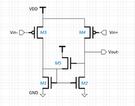
Recently I saw a differential pair architecture with a feedback mechanism but could not understand the role of the feedback transistor on the circuit performance. This cell is advised to use in a fully differential autozeroing comparator circuit as the amplification stage. Can someone explain the role of M5 transistor here?

Thanks
 

Attachments

  • diff_pair.png
    diff_pair.png
    50.4 KB · Views: 54
I guess the top mosfets are Pmos having a dot at the bias. Then the other 3 are Nmos. I'm running a simulation of the schematic however it doesn't seem to be a differential detector. It's not constructed like a conventional long-tail pair. M5 is configured so that the right-hand column (bias) influences the left-hand column. In turn this can affect the right-hand.

The amount of influence can be adjusted by changing voltage which supplies M5.
So the purpose may have to do with: a) changing gain of the incoming signal, or b) to balance the gains of common mode voltage so it can be cancelled more effectively.

Any adjustment shifts a DC component on Vout. I think that's the reason an 'auto-zeroing' circuit is advised. My simulation puts a series capacitor on the output similar to a garden-variety class A amplifier.
 
Hi BradtheRad,

Thank you for your response, actually I noticed I forget to put the dc current source on top. I created a test bench and put sinusoidal signals in the inputs (out of phase 1mV at 10kHz with 0.9V DC). After running a transient I noticed some difference on the drain currents of input PMOS transistors (M3 and M4) for the cases when M5 exists vs when it does not. Output voltages and DC operating points are almost same. I think M5 is injecting some current to the node where M1's and M2's gates are connected without changing the bias points. This additional injection of current may be helpful in one of the phases (autozeroing or comparison) when this is used in the comparator. But still not very clear for me.
--- Updated ---

If the circuit is sketched correctly, M5 is working as a clamp circuit limiting Vout.
Hi FvM, I also think it is kind of clamping but since the drain is connected directly to the Vdd and Vout seems to be not effected directly, yes Vout value is sensed via gate of M5 and M5 is turning on but it is just injecting some current to the M1-M2 gate node (see my previous response)
Regards
 

Attachments

  • with_M5.png
    with_M5.png
    91 KB · Views: 39
  • without_M5.png
    without_M5.png
    75 KB · Views: 41
Last edited:

LaTeX Commands Quick-Menu:

Part and Inventory Search

Welcome to EDABoard.com

Sponsor

Back
Top