Welcome to our site! EDAboard.com is an international Electronics Discussion Forum focused on EDA software, circuits, schematics, books, theory, papers, asic, pld, 8051, DSP, Network, RF, Analog Design, PCB, Service Manuals... and a whole lot more! To participate you need to register. Registration is free. Click here to register now.
for small signal model
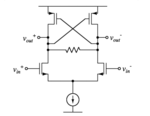
i just want to find the differential gain of this circuit, so either i can use the conventional superposition theorem and then get the differential and common mode gain, or draw the respective differential ad common mode half circuits and solve those.
Now i know while drawing the differential mode half circuit the middle point of the symmetric half circuit will be at 0v(fo small signal analysis case) so the R will be changed to R/2 but what will happen to the pmos's half circuit i am unable to draw that
I guess a half-circuit is made up of either the left-hand or right-hand column? In fact they cannot be evaluated individually. Each side affects what happens on the other side.
The cross-coupled Pmos create an effect similar to an RS flip-flop. If one Pmos turns on, it turns off the other Pmos. They tend to retain that state until a different Pmos is biased on or off. It's the basis for a memory cell.
That circuit is combined with your long-tail pair Nmos which create a differential amplifier. Their operation is not readily obvious. If one Nmos increases current flow then it reduces current flow in the other Nmos. The reason is because Ampere level in the current source shall stay the same.
The Nmos differential amplifier principle is not that different from the cross-coupled Pmos. However the latter arrangement is more like a 'snap action' when it changes state.
Question: Is there a chance the upper half of your circuit causes unexpected operation in combination with the lower half?
For small signal, since the circuit is symmetric we can consider the tail node to be ac ground. Then you have the NMOS transistor with source to ground. At the drain you have the loading. The resistor in-between the gates is r/2+R/2 and you can think of the middle point between the R/2 parts as being ac ground. The cross-coupled PMOS pair, looking differentially into it has a negative impedance of 2/gm, an again that total impedance can be thought of as -1/gm-1/gm with the middle point at ac ground. So, the load at the NMOS transistor drain is (R/2)||(-1/gm) to ac ground. This would be your half circuit. Of cource R/2 has to be bigger than abs(-1/gm), otherwise it will latch.
This site uses cookies to help personalise content, tailor your experience and to keep you logged in if you register.
By continuing to use this site, you are consenting to our use of cookies.