xiangx93
Newbie level 6
Hi,there! Recently I have been working on the design of inductor. My method is, first drawing an inductor in Cadence Virtuoso, and then getting its characteristics in ADS after import.
To verify the validity of my ADS simulation method, I'd like to compare the foundry model(simulated in Cadence, 55nm GlobalFoundry)with ADS simulation results and see if they match.
The comparison involves S-parameters(S11,S21),inductor, and resistance. Now my problem is, S21 and resistance between the two are a bit far from identical.
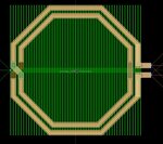
Take the following case for example(please refer to Inductor.JPG), it's a differential inductor made of three top metal layers, the patterned ground shield is down under made in a lower metal(i.e. M1).
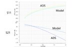
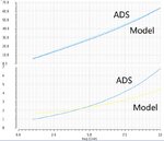
The comparison results are shown in Result_Comparison.JPG: it seems like the faster growth of parasitic resistance has caused a bigger insertion loss(i.e. S21), is that right?
In light of the difference, there are two settings I am really doubting about:
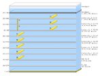
1)Substrate. Since I haven't found out the dielectric constants in the process document, I get these "average" values by calculation upon post-simulation capacitance extraction in plate capacitor model.Please refer to Substrate.JPG.Are there any apparent mistakes?
2)Ground connnection of patterned shield. I finish the ground connection by simply putting a pin over M1’s left edge and then connecting it to ground in the schematic view. I've found out the pin position can slightly affect the simulation results. Should there be any special handling on this?
To verify the validity of my ADS simulation method, I'd like to compare the foundry model(simulated in Cadence, 55nm GlobalFoundry)with ADS simulation results and see if they match.
The comparison involves S-parameters(S11,S21),inductor, and resistance. Now my problem is, S21 and resistance between the two are a bit far from identical.
Take the following case for example(please refer to Inductor.JPG), it's a differential inductor made of three top metal layers, the patterned ground shield is down under made in a lower metal(i.e. M1).
The comparison results are shown in Result_Comparison.JPG: it seems like the faster growth of parasitic resistance has caused a bigger insertion loss(i.e. S21), is that right?
In light of the difference, there are two settings I am really doubting about:
1)Substrate. Since I haven't found out the dielectric constants in the process document, I get these "average" values by calculation upon post-simulation capacitance extraction in plate capacitor model.Please refer to Substrate.JPG.Are there any apparent mistakes?
2)Ground connnection of patterned shield. I finish the ground connection by simply putting a pin over M1’s left edge and then connecting it to ground in the schematic view. I've found out the pin position can slightly affect the simulation results. Should there be any special handling on this?