Continue to Site

Welcome to EDAboard.com

Welcome to our site! EDAboard.com is an international Electronics Discussion Forum focused on EDA software, circuits, schematics, books, theory, papers, asic, pld, 8051, DSP, Network, RF, Analog Design, PCB, Service Manuals... and a whole lot more! To participate you need to register. Registration is free. Click here to register now.

Dielectric_oscillator_10_GHz

Status
Not open for further replies.

LeThalois

Newbie level 6
Joined
May 14, 2012
Messages
12
Helped
0
Reputation
0
Reaction score
0
Trophy points
1,281
Activity points
1,354
hello every one.

I find no words to describe my situation.

there is 2 months that I am designing a DRO oscillator in microstrip technology at 10 GHz

I tried the following figure, but in vain.
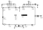
DRO.jpg

Please, help me, soon my academic defense and I have done nothing yet.

if you know a schema, a list of steps, I would be very happy even with a single encouraging word.

thank you with all my heart.
 

Well, that is a start.

I would do the following:
1) put a 50 ohm resistor to ground at the Vout port
2) remove the "DC Block 1" and put a port 1 and port 2 there.

I would then ask the forward gain and phase for a signal going thru the amplifier and DRO puck.

I would then trim the phase length of the transmission lines so that the round trip phase was 0 degrees, and the gain was at least 4 dB at the frequency of oscillation.

At that point, the circuit should oscillate, since you have satisfied the two conditions of oscillation.

You can simulate the oscillation is you have a non-linear simulator, or you can actually build the unit and test its oscillation.

You, of course, need an accurate model for the dielectric resonator puck, as well as the S parameters for the active device.

Once you get it oscillating, you should simulate the frequency pulling of the oscillator with changing output load at Vout, Frequency change as the round trip phase length is changed +/- 30 degrees, if a large signal model effects of power supply voltage change, etc.

You might change the puck Q or coupling and try to estimate the oscillator FM noise impact.
 
since this is for school, you should be able to impress the professor on your knowledge of the following:
https://en.wikipedia.org/wiki/Barkhausen_stability_criterion

And remember that all oscillators are LARGE SIGNAL devices, so the small signal S parameters for your active device will be a little off as the oscillations build up.
 
what do you think about this methode

1°-calculate K of a tnt of ower choice

transi.jpg

2°-we make a feed back circuit that make S11>1 or S22>1 like this

with_feed.jpg

3°-then resonnate the input port like this

complet.jpg

and is this available in loop feed back parallel ? this is the document that i use **broken link removed**

thank you a lot
 

Status
Not open for further replies.

Part and Inventory Search

Welcome to EDABoard.com

Sponsor

Back
Top