Continue to Site

Welcome to EDAboard.com

Welcome to our site! EDAboard.com is an international Electronics Discussion Forum focused on EDA software, circuits, schematics, books, theory, papers, asic, pld, 8051, DSP, Network, RF, Analog Design, PCB, Service Manuals... and a whole lot more! To participate you need to register. Registration is free. Click here to register now.

Designing Discrete Differential Amplifier

Status
Not open for further replies.

ssquared

Junior Member level 3
Joined
Jun 6, 2015
Messages
30
Helped
1
Reputation
2
Reaction score
1
Trophy points
8
Activity points
213
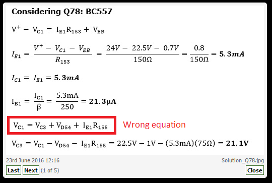
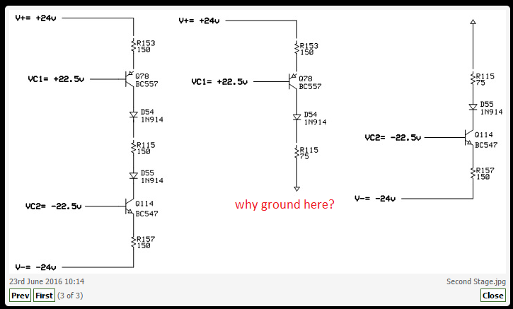
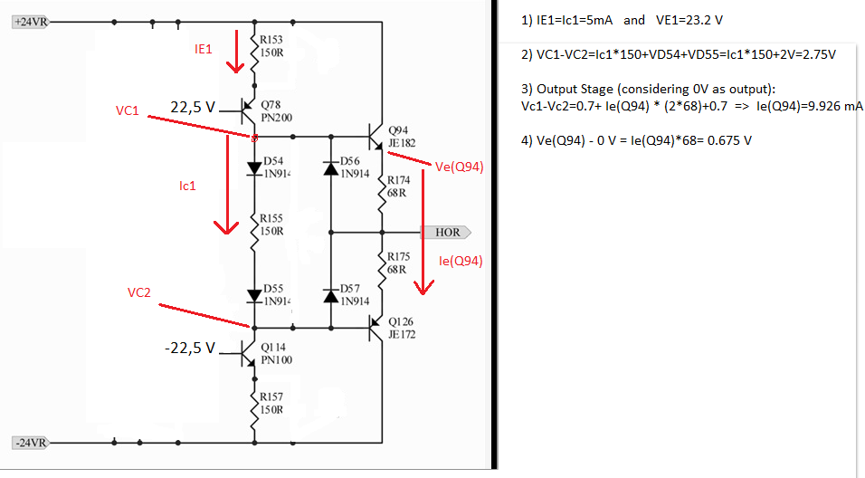
I am trying to analyse a discrete differential amplifier circuit by answering some question. I have done the analysis of the input stage, I would appreciate if I can get some feedback on my approach.

Circuit.jpg

Input Stage.jpg

Input Stage_PNP.jpg

- - - Updated - - -

Solution_1.jpg

Solution_2.jpg

Solution_3.jpg

Solution_4.jpg

Solution_5.jpg

Solution_6.jpg

Solution_7.jpg

Solution_8.jpg

Solution_9.jpg

Solution_10.jpg

Solution_11.jpg

Solution_12.jpg
 

You have split the long-tail pair into separate amplifiers, for individual analysis (so it appears). However, each side influences the other. It's an effect caused by voltage on the tail resistor, the common resistor. Notice that if you increase current going through one side, it reduces current level in the other side.

This creates the distinctive behavior in the differential amplifier. In a manner of speaking, the two sections each bid for their share of the tail resistor. It becomes difficult to separate the two sections.
 

Thanks for your reply. I think it is fine to split the differential amplifier for easy analysis. It can be seen that the value of the tail resistor has been doubled for each of the section. I read this from somewhere but I can really remember now.

My doubt is with the analysis of the splitted circuits
 

I have watched the analysis of Q111 and in my view is correct (as an approximation..). the others are done in the same manner.

Q78 in the before next-to-last attachment is not correct. IE1*R153=V+ - VE1 (not VC1) . So as it is a PNP, then the Emitter is 0.7 V higher than the base, so it should be 24V - (22.5+0.7) V
 

@CataM. Thank you very much. But I think for Q78. The expression should be V+ - Vc1= IE1*R153 + VBE
where Vc1 is the collector voltage from the input (first) stage.

What do you think?
 

As mentioned, Q78/Q114 current is calculated wrong. The voltage drop across emitter resistors is 0.8 instead of 1.5 V. Thus current is 5.33, not 10 mA.

I wonder about the practical usefulness of the amplifier. It has only very poor common mode rejection.
 

@CataM and FvM. Thanks, I just corrected it as you can see here. I have also done the calculation for the collector voltage of Q78Solution_updated_1.jpg
 

The Q78 collector voltage calculation isn't right. The difference Ic,Q78 - Ic,Q114 is driving a high impedance node. You can assume that both current magnitudes are exactly equal and cancel each other and the amplifier has zero output voltage. But in a real amplifier there will be small asymmetry and the output jumps to either high or low. Negative feedback is required to set a stable output voltage.
 

@FvM. Thanks very much for the explanation. I have done the calculations in Q78 again as you can see in the attachment below. I have also attached the calculations for Q114. Solution_Q78.jpgSolution_Q114.jpgPlease I would appreciate if you can give me some feedback

- - - Updated - - -

This is my approach, I divided this part into two as shown in the figure
Second Stage.jpg
 
Last edited:

Q78 emitter current is incorrect, it is 5mA as in post #7 and post #6. I have just said that it is correct to say VEB instead of VBE but the calculation is correct. In your post #7, just change VBE with VEB and nothing more for the emitter current.

On post #10, your splitted circuits are not correct in my view (you can not do that...). Ic of Q78 and Ic of Q114 are equal.
 

@CataM. Thanks very much. I have corrected the calculations already as you can see here. The emitter current is 5.3mA.
Solution_Q78.jpg
Solution_Q114.jpg


I am a bit confuse with the analysis of the output stage (Q94 and Q126), shown below
Output Stage.jpg

Here are the calculations
Solution_Q94.jpg
Solution_Q126.jpg
 

I wanted to divide the circuit into two to make it easy for the calculation. I realized it is wrong. I have tried to come out with a different equation

Vc1 - Vc2 = VD54 + IcR115 + VD55
 

@CataM, Thank your very much for your assistance.

At least I am done with the current and voltages. Now my next task is to calculate the open loop output impedance at 1kHz
 
Last edited:

I am trying to calculate the open loop differential gain of the circuit.

From my understanding, the gain for the amplifier containing Q111 and Q112 will be calculated as follows: Av = Rtot/2re, where Rtot is the total resistance of R117 and the input resistance of Q78 which is Rin. So the gain Av = Rtot/500 ohms. If hFE for Q78 is 250, Rin = hFE*R115 = 250(150) = 37500 ohms. So Rtot = R117//Rin = 10714.3 ohms. Using this value the gain Av = 10714.3/500 = 21.4

I don't know if I am approaching it the right way.
 

I just used the formula: Rin = beta*(R153 +re) but I neglected re. So I just used Rin = beta*R153
 

Fine with Re but 2 things:

1) In post #17 it says beta*R115
2) In my approach is (1+beta)*R153

Did you approximate 1+beta to just beta ?
 
Status
Not open for further replies.

Similar threads

Part and Inventory Search

Welcome to EDABoard.com

Sponsor

Back
Top