Continue to Site

Welcome to EDAboard.com

Welcome to our site! EDAboard.com is an international Electronics Discussion Forum focused on EDA software, circuits, schematics, books, theory, papers, asic, pld, 8051, DSP, Network, RF, Analog Design, PCB, Service Manuals... and a whole lot more! To participate you need to register. Registration is free. Click here to register now.

Delay of a 32:1 multiplexor

Status
Not open for further replies.

dll_fpga

Full Member level 3
Joined
Mar 9, 2011
Messages
185
Helped
19
Reputation
38
Reaction score
21
Trophy points
1,298
Location
kerala,India
Activity points
2,416
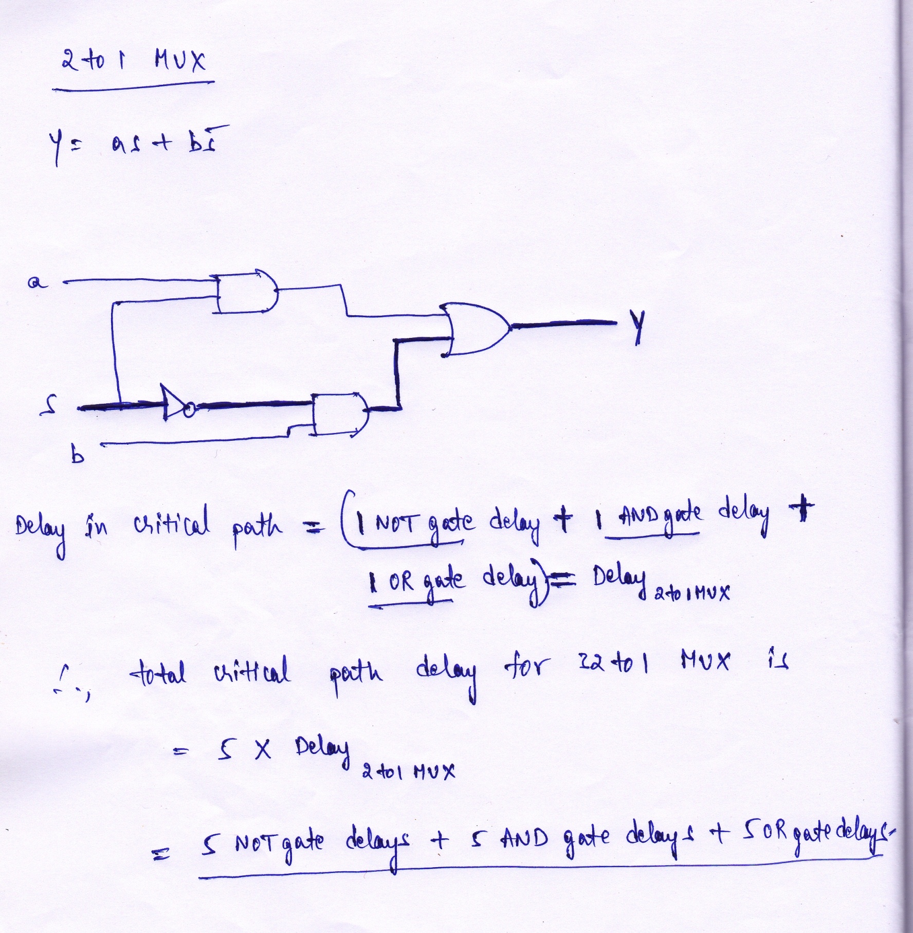
what will be the delay of a 32 :1 generic multiplexer
Please provide the equivalent gate delay.

eg: say(10 gate delays)...
 

A 32 to 1 Multiplexer is constructed in 5 stages of 2 to 1 MUXes(16 in stage 1, 8 in stage 2 and so on till 1 in 5th stage)

So you'll have 5 times the delay of a single stage (considering parallel delays in each stage to be the same)

The result is shown in image below.


All the best.

- - - Updated - - -

Usually the delay of NOT gate will be considered as 1 unit while delays of AND gate and OR gate will be 2 or 3 units of time
 
thanks prasanth...for deriving from the basics

- - - Updated - - -

also does the synthesis/STA tool follows this approach?
of deriving N:1 mux using 2:1 multiplxers?
Is the delay calculation shown above, accurate from the practical point of view?
 

Yes. Thats the functional representation of a multiplexer. So the basic equations wont change and hence the timing analysis too.

But I dont think that the results are accurate and as expected. You got to do it and cross check approximately.

Also it depends on the style(CMOS) of MUX Design like static CMOS style, Dynamic CMOS stlyle, Domino Logic style of design.

I would like to know about your further proceedings and results estimated.

All the best.
 

Maybe the OP is only interested in the data path delay?
That delay will be lower if the mux is implemented as 32 AND gates (one per input) followed by a 32-input OR-gate.
The data path delay will be 1 AND gate delay + 5 OR-gate delays, or lower if OR gates with more than 2 inputs can be used.
The delay from a control input change must also include the needed "one-hot" decoder.

The previous delay calculation included the inverters for the select ("s") signals, so it was really the delay for a control input change.
It was also not correct since the critical path for the complete 32-input multiplexer will have only one inverter, in the first stage with 16 2:1 multiplexers.
The inverters in the other stages are not in the same path (the outputs from the first stage will not go through another inverter).
 

Thanks Std_match.

I dint think of those inverters in other stages.

Yes, in my explanation the total data path delay will be
5 AND Gate Delays + 5 OR Gate Delays + 1 NOT Gate Delay. I considered fanin=2.

If i use 32 AND gates with fanin=5, the delay will be less as you mentioned.
 

Status
Not open for further replies.

Part and Inventory Search

Welcome to EDABoard.com

Sponsor

Back
Top