Continue to Site

Welcome to EDAboard.com

Welcome to our site! EDAboard.com is an international Electronics Discussion Forum focused on EDA software, circuits, schematics, books, theory, papers, asic, pld, 8051, DSP, Network, RF, Analog Design, PCB, Service Manuals... and a whole lot more! To participate you need to register. Registration is free. Click here to register now.

dc bias point of power amplifier

Status
Not open for further replies.

vahidnoori

Junior Member level 2
Joined
Dec 25, 2013
Messages
21
Helped
0
Reputation
0
Reaction score
0
Trophy points
1
Activity points
137
hi.
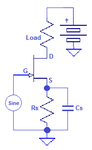
i am decided to design power amp. but i don't know how can i determine the bias point from ID-VDS curve ,is there good document that explain design of dc biasing of PA ? my schematic and my curve is attached.

thanks.


You do not have a power amplifier. Instead you have a Jfet short circuiting the power supply on each half cycle of the input like a rectifier.
The Jfet has no load.
 

You do not have a power amplifier. Instead you have a Jfet short circuiting the power supply on each half cycle of the input like a rectifier.
The Jfet has no load.

i am beginning. how can i place load and bias resistor? in this circuit how can set load resistor , ... to determine bias point to make for example A class power amp .
thanks
 

A load can connect between the drain of the Jfet and the positive power supply. It will have AC and DC in it.
The gate of the Jfet must be negative compared to the source which can be made by adding a resistor between the source of the Jfet and 0V.
Doo Eet like this:
 

Attachments

  • Jfet class-A amplifier.png
    Jfet class-A amplifier.png
    3 KB · Views: 133

hi
i did it. but the current (ID) decries .generally i don't know how can determine the bias point from ID-VDS curve
please help me .the pic attached.


The datasheet for the Jfet shows a maximum allowed Vds voltage of 15V and recommends a maximum Vds of 6V but your circuit has a maximum voltage of 70V!
The datasheet shows an RF amplifier circuit. Why don't you use it?
 

The datasheet for the Jfet shows a maximum allowed Vds voltage of 15V and recommends a maximum Vds of 6V but your circuit has a maximum voltage of 70V!
The datasheet shows an RF amplifier circuit. Why don't you use it?

i try it by max VDS in 7 but the max ID=.06mA ,what should i do ? why he current is little .
how can i determine my class of PA?
 

i try it by max VDS in 7 but the max ID=.06mA ,what should i do ? why he current is little?
The datasheet for the Jfet shows that when the gate bias voltage is low then the drain-source current is hundreds of mA.
But you have a drain load resistor that is such a high value of 1k that the MAXIMUM current with a 7V supply is only 7mA.

how can i determine my class of PA?
You need to learn that a linear transistor that conducts all of the waveform it is class-A, when it conducts only half the waveform it is class-B and when it conducts only part of the waveform it is class-C.
 

yes i know it how can i set my PA on class A for exp.in other word where and how should i place the bias point on ID-VDS curve that make the transistor work on class A?
what is the location of bias point on ID_VDS curve exactly ?
thanks.
 
Last edited:

For class-A, the bias point of a Jfet is where its output can swing an equal amount towards saturation and towards cutoff.
If there is no series source resistor then the drain quiescent voltage is about half the supply voltage (but the second harmonic makes one direction a little more amount than the other direction).

excuse me for my several questions.but can u explain the bias point in ID-VDS curve or is there document that explain it exactly ?
 

The class-A bias point of a Jfet without a series source resistor is when its quiescent drain voltage is almost half the supply voltage, so the drain voltage can swing equally up and down by a signal.
I said that in my last post.
 

The class-A bias point of a Jfet without a series source resistor is when its quiescent drain voltage is almost half the supply voltage, so the drain voltage can swing equally up and down by a signal.
I said that in my last post.

is there any good document for it?
 

Status
Not open for further replies.

Similar threads

Part and Inventory Search

Welcome to EDABoard.com

Sponsor

Back
Top