nelsonys
Member level 4
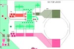
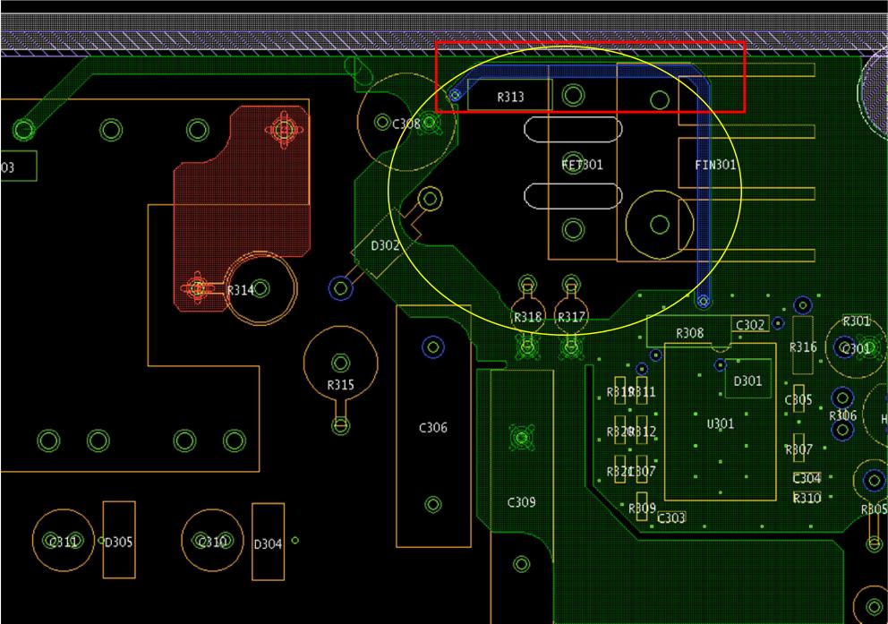
Please refer to the attachment. Sorry for the low quality image.
This is part of the flyback converter circuit. As you can see, the blue trace is the path connected to the gate of the FET through R313 to send fast PWM control signals to the FET. I have added GND (green) path at the upper part of the blue trace, highlighted in red rectangle to act as the nearest return for the PWM signal in order to minimize the current loop. But I have also created another ground loop, highlighted in yellow circle which I do not know whether there is any impact to the circuit (loop antenna effect?)
Please advice on this layout.
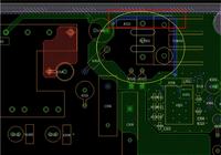
") )
)