Continue to Site

Welcome to EDAboard.com

Welcome to our site! EDAboard.com is an international Electronics Discussion Forum focused on EDA software, circuits, schematics, books, theory, papers, asic, pld, 8051, DSP, Network, RF, Analog Design, PCB, Service Manuals... and a whole lot more! To participate you need to register. Registration is free. Click here to register now.

[SOLVED] Create EM Substrate for CMOS tech Momentum RF

Status
Not open for further replies.

fred3991

Member level 1
Joined
Nov 26, 2020
Messages
33
Helped
0
Reputation
0
Reaction score
0
Trophy points
6
Activity points
615
Hello!

I want to create an EM substrate for electromagnetic simulation in Keysight ADS and would like some advice on how this can be done correctly.

Initially I only had the information from the Desigh Rule Manual(DRM) for CMOS technology.
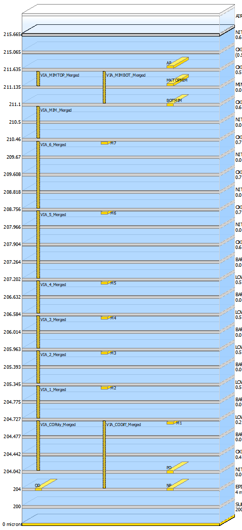
Using the information on the internet and the substrate files for ADS other technologies (.ltd files) I created the following structure
1647717235756.png


The parameters of metal layers (thickness and conductivity) and dielectric layers (thickness and dielectric constant) were taken from the DRM.
I even found information about "derived layers" in ADS and created a merging of metal vias into one polygon (to reduce the simulation time).. https://muehlhaus.com/archives/1411

For this CMOS technology, there are real measurements of elements made at the sonde station with a vector network analyzer (microstrip lines, coils and MIM capacitors).
After several variations of selecting the thickness of dielectrics, dielectric constant, conductivity of materials, I began to get a little close results EM simulation (Momentum RF).
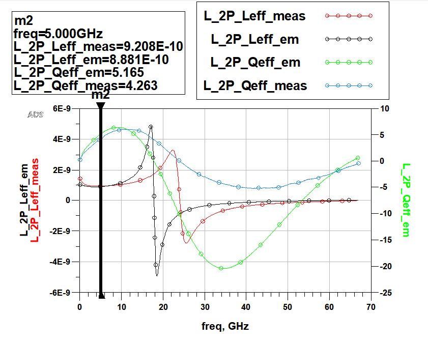
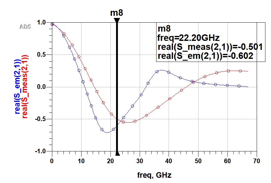
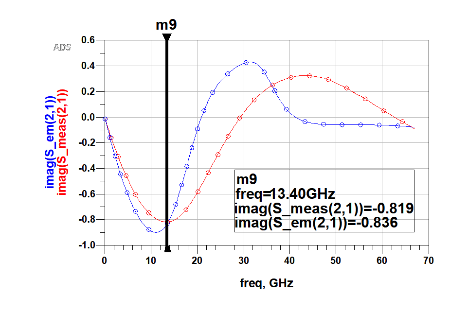
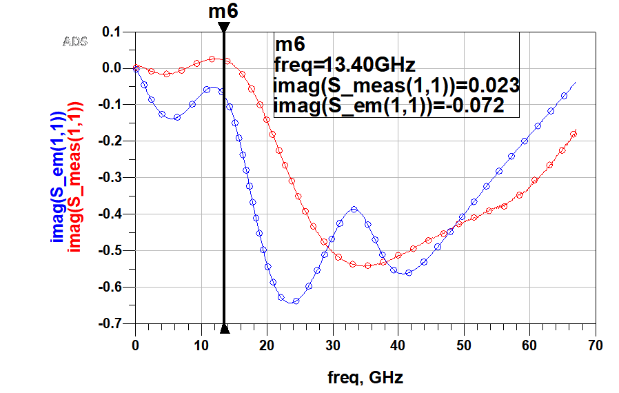
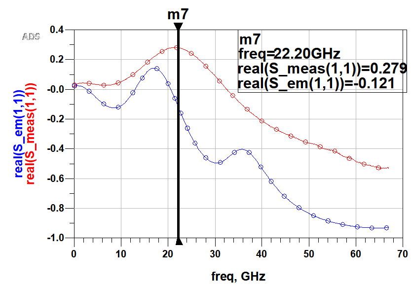
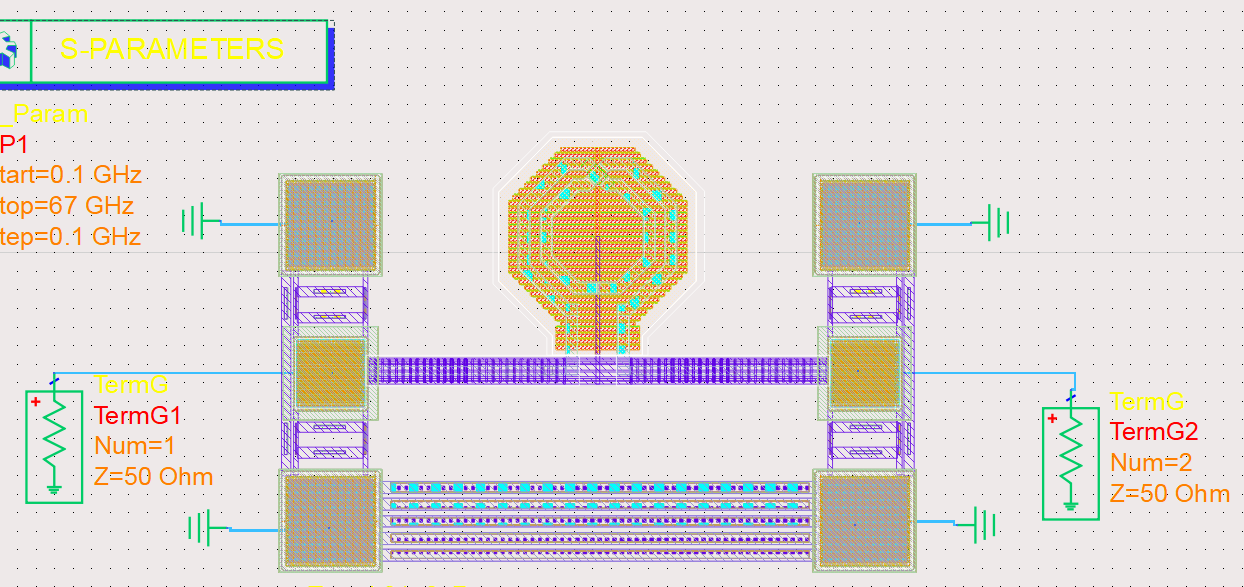
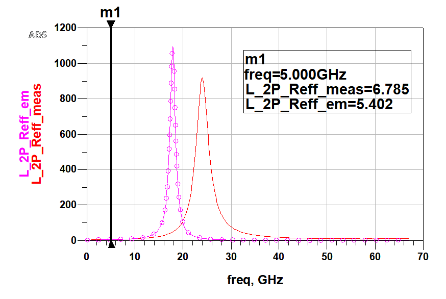
For example here - to check the EM substrate (without sparing the CPU power and my time 🤪) I tried to simulate the inductor coil together with the pads and lines and these are the results I got.
1647717404009.png


1647717501966.png
1647717488937.png


Obviously, now the substrate has too high dielectric constant (Self Res Freq should be shifted to the right).
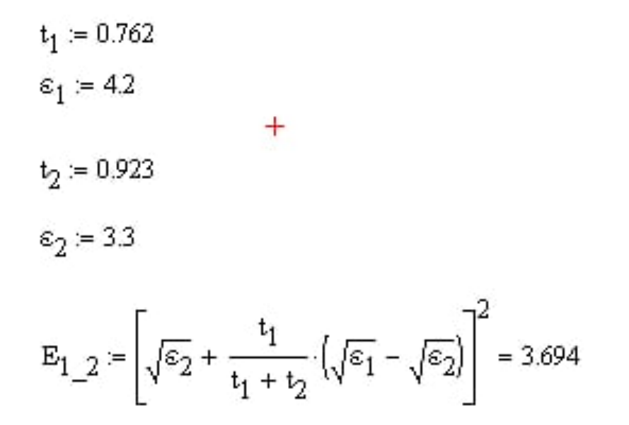
Also, as far as I know, many dielectric layers can be combined by one equivalent layer.

(by this formula?)
1647717776612.png


1647717512331.png
1647717576634.png


1647717658197.png
1647717678916.png


My questions are as follows:

What additional structures need to be fabricated and measured to accurately estimate the substrate parameters? (Perhaps baluns, line segments in individual metal layers?)

Is there any algorithm or key points for creating an EM substrate? Or is it only possible to change the substrate parameters and simulate a very large number of times until an acceptable result is obtained? only a brute-force search 😱?)
In other words, there is no clear answer and I have to rely only on my own experience?
 

Solution
The agreement on SRF is indeep unexpected, that should agree much better. Capacitance for SRF is a combination of C between the turns and C to the substrate below.

One possible issue for C between the turns is modelling of the top layer passivation: if you have thick top metal and assume that these conductors are fully embedded in dielectric (=planar stackup modelling) that will over-estimate C if real passivation is conformal with much air between the traces. Not sure about CMOS, but in SiGe I often see those thick top metals (some microns).

~~

To check C to the substrate, you can model a large square plate, with port reference at bottom of the substrate, and compared results to the shunt C specification in process spec. That will...
The agreement on SRF is indeep unexpected, that should agree much better. Capacitance for SRF is a combination of C between the turns and C to the substrate below.

One possible issue for C between the turns is modelling of the top layer passivation: if you have thick top metal and assume that these conductors are fully embedded in dielectric (=planar stackup modelling) that will over-estimate C if real passivation is conformal with much air between the traces. Not sure about CMOS, but in SiGe I often see those thick top metals (some microns).

~~

To check C to the substrate, you can model a large square plate, with port reference at bottom of the substrate, and compared results to the shunt C specification in process spec. That will give an idea if your stackup is correct for shunt C.

~~

Sometimes measurements are not correct, so try to double check that also. Having some error in shunt C is not unusual, even if on-wafer-cal was done.

~~

For effective permittivity, calculation depends on direction also. I have attached my calculations below:
dielectric_merge.png


~~

The appnote on via merging was created when ADS had no built-in via array merging. Today, the recommended method is to use ADS via array merging.

via_array_merge.png

--- Updated ---

Is there any algorithm or key points for creating an EM substrate? Or is it only possible to change the substrate parameters and simulate a very large number of times until an acceptable result is obtained? only a brute-force search 😱?)
In other words, there is no clear answer and I have to rely only on my own experience?

I have created many EM stackups for RFIC technology and my advice is: use data from process specification. It is very dangerous to tweak values for agreement between EM and measurement. There are too many error sources in measurement, and user generated modelling error in EM, so you will never get reliable stackups that way. If there is one thing that you can trust, it is the process documentation.
 
Last edited:

Solution
The agreement on SRF is indeep unexpected, that should agree much better. Capacitance for SRF is a combination of C between the turns and C to the substrate below.

One possible issue for C between the turns is modelling of the top layer passivation: if you have thick top metal and assume that these conductors are fully embedded in dielectric (=planar stackup modelling) that will over-estimate C if real passivation is conformal with much air between the traces. Not sure about CMOS, but in SiGe I often see those thick top metals (some microns).

~~

To check C to the substrate, you can model a large square plate, with port reference at bottom of the substrate, and compared results to the shunt C specification in process spec. That will give an idea if your stackup is correct for shunt C.

~~

Sometimes measurements are not correct, so try to double check that also. Having some error in shunt C is not unusual, even if on-wafer-cal was done.

~~

For effective permittivity, calculation depends on direction also. I have attached my calculations below:
View attachment 175001

~~

The appnote on via merging was created when ADS had no built-in via array merging. Today, the recommended method is to use ADS via array merging.

View attachment 175000
--- Updated ---


I have created many EM stackups for RFIC technology and my advice is: use data from process specification. It is very dangerous to tweak values for agreement between EM and measurement. There are too many error sources in measurement, and user generated modelling error in EM, so you will never get reliable stackups that way. If there is one thing that you can trust, it is the process documentation.


Thank you so much for your advices!

About the top metal - yes, according to the DRM it uses a thick layer of Aluminum.
And to be honest, this is the moment that raises the most questions for me.
Could you please explain more about the C and the top metal?

A MIM capacitor, (MIMTOP and MIMBOT) is included between the top metal Alumina and the M7 thick metal (Copper 0,9µm).
In addition, the documentation states that where there is a PAD Open (contact pads or inductance coil as in the figure below), the top Aluminum metal is in contact with metal 7 (No Physical Vias).
1647796259245.png
1647796290418.png


Here is 3D view at this place (coil)

1647796443678.png
1647796575653.png


I don't quite understand how to describe this in the LTD file correctly so that everything is as accurate as possible ( MIM capacitor between the Al and M7 layers and the Al-M7 contact where the coil is.
1647797090665.png


Would it be possible to change the capacitance at this place if the dielectric layers at this place were set very thin or with a very low dielectric value?
Or what can be done in this situation to create an LTD file and EM simulation?
 

The combined case with/without MIM is difficult to configure indeed. For a layer-oriented planar solver like Momentum, such non-planar structures are difficult to capture.

I would propably keep it simple and create a stackup without MIM first. That should model your inductor case and many other cases, except the special cases MIM and pad open area.

Regarding SRF, check if your stackup models the conformal coating for thick Al layer properly. If that coating is thin in reality, just a conformal coating above the Al layer, you must NOT model this as Al layer fully embedded in that dielectric. Instead, I recommend to calculate an effective permittivity then, which is valid in horizontal direction between the inductor turns for your actual gap width in this inductor. Does SRF agree better now?

~~

Would it be possible to change the capacitance at this place if the dielectric layers at this place were set very thin or with a very low dielectric value?

I don't understand this part of your question. Do you mean an equivalent material to mimic the MIM, or what does this refer to ?
 

The combined case with/without MIM is difficult to configure indeed. For a layer-oriented planar solver like Momentum, such non-planar structures are difficult to capture.

I would propably keep it simple and create a stackup without MIM first. That should model your inductor case and many other cases, except the special cases MIM and pad open area.

Regarding SRF, check if your stackup models the conformal coating for thick Al layer properly. If that coating is thin in reality, just a conformal coating above the Al layer, you must NOT model this as Al layer fully embedded in that dielectric. Instead, I recommend to calculate an effective permittivity then, which is valid in horizontal direction between the inductor turns for your actual gap width in this inductor. Does SRF agree better now?

~~


I don't understand this part of your question. Do you mean an equivalent material to mimic the MIM, or what does this refer to ?
Right now I have the total thickness between Al and M7 (0,5 + 0,035 + 0,6 + 0,04) - In order to place the MIM capacitor there.
Because of the large thickness of the dielectric there may be additional capacitance, that shouldn't be there.
1647803050761.png


If I make the thicknesses of these dielectric layers very thin (~0.01 um for example) will this help to reduce the "extra" capacitance, and get a better SRF match?

I agree that perhaps 2 substrate files should be used - one for coil modeling and metallization, and one for MIM capacitor. But I wouldn't want that, because in design very often the L and C are placed in the same layout, and I would like to keep the ability to simulate them at the same time.
 

If I make the thicknesses of these dielectric layers very thin (~0.01 um for example) will this help to reduce the "extra" capacitance, and get a better SRF match?

Ultra thin layers can lead to numerical issues.

Not sure if I understand your technology correctly. Is the "normal" case in the inductor trace region to have some distance between M7 and Al, and "pad open" creates a connection similar to a via?

~~

As mentioned before, you have embedded the Al layer completely into oxide: oxide thickness is 0.5 + 2.93µm, and that also covers the gaps between turns am layer Al. In reality, there are gaps with air, and you over-estimate capacitance.

Let me use a picture from another technology, to explain what I mean:
foundry_stackup.png
 

Ultra thin layers can lead to numerical issues.

Not sure if I understand your technology correctly. Is the "normal" case in the inductor trace region to have some distance between M7 and Al, and "pad open" creates a connection similar to a via?

~~

As mentioned before, you have embedded the Al layer completely into oxide: oxide thickness is 0.5 + 2.93µm, and that also covers the gaps between turns am layer Al. In reality, there are gaps with air, and you over-estimate capacitance.

Let me use a picture from another technology, to explain what I mean:
View attachment 175017
I think this picture is as similar as possible to what I have in the DRM

XXXX

PadOpen layer - serves as a sort of marker - Al layer is applied directly to M7. In other cases Al and M7 are isolated by dielectric
Not sure if PadOpen layer can be considered - as metal layer over M7 or as Via between Al and M7?

Also shown is the metal stack of one coil turn - it is a metal stack from Al to M5 - underpass layer in M4.

XXXX

I understand your point about the "extra" capacity.
I will try to redo the LTD file with your notes in mind.


By the way, I tried to repeat Deembeding L-2L using only EM results, (I simulated L with pads, 2L with pads, and inductance coil with pads, and separately coil without lines and pads)


Comparing the EM results for the coil separately, and the deembedded EM coil I found out that the deembedding is not quite perfect either.

1647872031093.png

1647872066439.png


You can see that the S-parameters after ~20GHz start to differ a lot. Also the SRF is different.

Could it be due to an incorrect substrate?

Or is this normal for the L-2L deembedding method ?

Perhaps there is a more advanced method of L-2L deembedding to get a more accurate match?

Can the shield under the L lines affect the deembedding? It might be worth repeating deembeding without the M1 shield under the L lines....
 
Last edited:

Not sure if PadOpen layer can be considered - as metal layer over M7 or as Via between Al and M7?

I would model that as a via, to connect Al and M7. Layer Al and M7 separated by 640nm oxide then, as shown in your cross section.

(We don't include the "valley" in Al at PadOpen then, but that's not an issue)

Or is this normal for the L-2L deembedding method ?
Let's do some math: we have 45GHz SRF at 600pH inductance. I calculate parallel C as 21fF from these values.

For measurements from clients, I have seen measurement uncertainty in shunt C of several fF per port. That would be enough to explain SRF shifts as you have observed.
But I really can't discuss more details, because that stuff is under NDA and because I'm not an expert in these on-wafer measurements.
--- Updated ---

~~

I think you better remove the detailed cross section from your last post, to avoid NDA trouble with the foundry.
 

I would model that as a via, to connect Al and M7. Layer Al and M7 separated by 640nm oxide then, as shown in your cross section.

(We don't include the "valley" in Al at PadOpen then, but that's not an issue)


Let's do some math: we have 45GHz SRF at 600pH inductance. I calculate parallel C as 21fF from these values.

For measurements from clients, I have seen measurement uncertainty in shunt C of several fF per port. That would be enough to explain SRF shifts as you have observed.
But I really can't discuss more details, because that stuff is under NDA and because I'm not an expert in these on-wafer measurements.
--- Updated ---

~~

I think you better remove the detailed cross section from your last post, to avoid NDA trouble with the foundry.

This image of the stack is not from the DRM)

This is from open source https :// tel.archives-ouvertes.fr/tel-00445302/file/ChapterIII.pdf

But it's very similar to what I have)
 

I would model that as a via, to connect Al and M7. Layer Al and M7 separated by 640nm oxide then, as shown in your cross section.

(We don't include the "valley" in Al at PadOpen then, but that's not an issue)


Let's do some math: we have 45GHz SRF at 600pH inductance. I calculate parallel C as 21fF from these values.

For measurements from clients, I have seen measurement uncertainty in shunt C of several fF per port. That would be enough to explain SRF shifts as you have observed.
But I really can't discuss more details, because that stuff is under NDA and because I'm not an expert in these on-wafer measurements.
--- Updated ---

~~

I think you better remove the detailed cross section from your last post, to avoid NDA trouble with the foundry.

I think this is the best that can be achieved at this moment)
Thanks again for your advices)

-Coil
image_2022-03-28_21-24-14.png


MIM Cap

image_2022-03-28_21-25-14.png


Line
image_2022-03-28_21-26-13.png
 

Status
Not open for further replies.

Part and Inventory Search

Welcome to EDABoard.com

Sponsor

Back
Top