Continue to Site

Welcome to EDAboard.com

Welcome to our site! EDAboard.com is an international Electronics Discussion Forum focused on EDA software, circuits, schematics, books, theory, papers, asic, pld, 8051, DSP, Network, RF, Analog Design, PCB, Service Manuals... and a whole lot more! To participate you need to register. Registration is free. Click here to register now.

coupler loose ends to finish the design

Status
Not open for further replies.

antenna_beginner

Member level 2
Joined
Feb 11, 2017
Messages
47
Helped
0
Reputation
0
Reaction score
0
Trophy points
6
Activity points
363
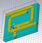
Hello , i am trying to implement a tandem coupler from the attached article. i have built cst the schematics as shown in the attached photo, but i have a few points in the schematics which are problematic to implement,which i signed with the red marker.
1.how to make this thin wire bridge over to port2?

2.how to make the ressistor connected to ground, iknow there is a lumped emelent in which i can define a ressistance but i am not sure if its connected to the ground or not

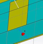
3. i have created a ground plane bellow the dielectrics , i have defined a waveguide port a straight rectancle at the size of the strip width, as shown in the attached photo,is the size of the port correct ,because i know that that we need to do it extra wide ,if you caould say the intutition of the port size to use ?

Thanks

Capture.JPG
View attachment 01390982.pdf
 

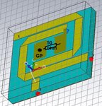
Hello, this square with a circle in the center was accomplished by making a hole and connecting the squere to the ground plane via a cilinder between them?
how did you see that this coupler has a hybrid properties 90 percent phase shift between the "through" and "coupled" ports ?

Thanks
 

i have constructed the structure and tried to run it
but it gives me the following error for all ports "the discrete edge port 1 is inside perfect conducting material. Please check the element location."

i have increased the location the ports are touching the patch the ground plane, also i tried to increase the accuracy ,but its not solving this error, what could solve it?

Thanks
capture2.JPGCapture3.JPG
 

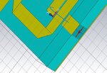
Hello , i have a problem with the ports, first i tried ports like you use between to points one point on te edge of surface edge of the ground plane and another in the patch.
it gave me "The discrete edge port 1 is inside perfect conducting material"

i tried another thing where i select the whole line at the edge of the patch and the other selection is the whole upper ground plane,and it gives me
"face elements touches boundary at xmin" as shown in the photos bellow.
what is the reason ?
Capture.JPGcapture2.JPG
Thanks
 

78.jpg....

- - - Updated - - -

79.jpg,,,,see it...!!!!
 

Hello , i implemented the ressistor as you said . i succeeded running it, but i get a phase shif of 100 degrees instead of 90, how can i improve the situation?

Thanks
Capture_phase shift.JPG
 

Status
Not open for further replies.

Part and Inventory Search

Welcome to EDABoard.com

Sponsor

Back
Top