AvocadoHead
Newbie
Hello, i need some insight on how to place waveguideports.
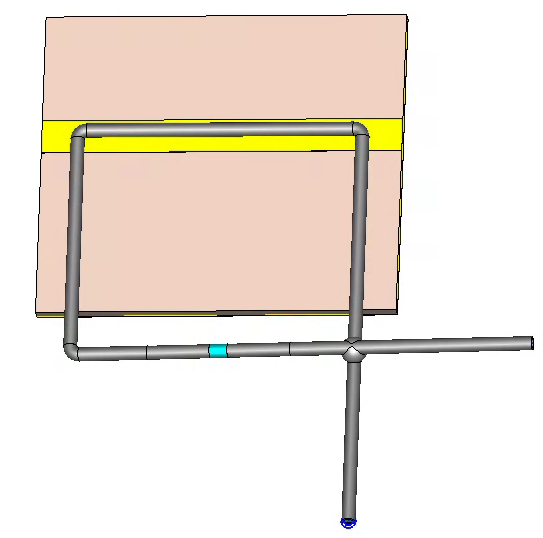
The following is a simplified model of what i am examinating.

This model consists of a microstrip (yellow) on a pcb (light brown) with groundplate (not visible in this view)
Above the microstrip and pcb i placed a capillary in the form of a square which is connected to itself with some solder at the bottom right intersection.
Now placing some waveguideports for the microstrip is the easy part and is described in detail here .
My question is how do i have to design and where do i have to place a waveguideport in order to get a special property of this model. This property is the line impedance im looking for
Similar to the line impedance of the microstrip i want to know what the lineimpedance of the capillary is. This turns out to be quite a confusing untertakeing because the results changes depending on how and where the port is placed.
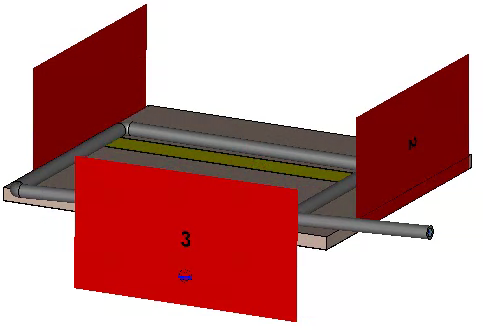
My current setup looks as follows:

Port 1&2 are for the micro strip and 3 is for the capillary.
The mesh is tetrahedral
I'm using the frequency domain solver
Excitation is on port 1 only, besides the line impedance the s-parameters are also very important
Frequency range is 0.1GHz - 1 GHz
I would like to hear some advice from experienced users
The following is a simplified model of what i am examinating.
This model consists of a microstrip (yellow) on a pcb (light brown) with groundplate (not visible in this view)
Above the microstrip and pcb i placed a capillary in the form of a square which is connected to itself with some solder at the bottom right intersection.
Now placing some waveguideports for the microstrip is the easy part and is described in detail here .
My question is how do i have to design and where do i have to place a waveguideport in order to get a special property of this model. This property is the line impedance im looking for
Similar to the line impedance of the microstrip i want to know what the lineimpedance of the capillary is. This turns out to be quite a confusing untertakeing because the results changes depending on how and where the port is placed.
My current setup looks as follows:
Port 1&2 are for the micro strip and 3 is for the capillary.
The mesh is tetrahedral
I'm using the frequency domain solver
Excitation is on port 1 only, besides the line impedance the s-parameters are also very important
Frequency range is 0.1GHz - 1 GHz
I would like to hear some advice from experienced users