Continue to Site

Welcome to EDAboard.com

Welcome to our site! EDAboard.com is an international Electronics Discussion Forum focused on EDA software, circuits, schematics, books, theory, papers, asic, pld, 8051, DSP, Network, RF, Analog Design, PCB, Service Manuals... and a whole lot more! To participate you need to register. Registration is free. Click here to register now.

Confusions in characteristic impedance calculations

Status
Not open for further replies.

asimlink

Full Member level 1
Joined
Jun 24, 2009
Messages
96
Helped
12
Reputation
24
Reaction score
12
Trophy points
1,288
Location
Islamabad
Activity points
2,288
Hi,

I am doing a board around xilinx virtex7 fpga in which i need to rout traces for upto 10~15Gbps GTH interfaces. I was looking through the pcb trace width and other parameters defined in xilinx virtex-7 evaluation board (V707) pcb stack [1].
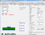
And I am using saturn pcb toolkit to compute characteristic impedance for single ended trace. But i get error that suggests T/H is an invalid input. Please refere to image [2] to see this error message produced by saturn toolkit.
I am doing this excercise as I need to change the material to Megtron-4 for my pcb and I offcourse need to adjust trace widths for single ended and differential signals for my design. Before actually doing this i wanted to validate the pcb trace width, clearance, heigh and copper widths used in Xilinx Virtex 7 (707 Evaluation board) .

Questions:
1. Can someone suggests if the pcb stack defined for v707 board is correct, then why saturn tool kit gives T/H error?
2. The characteristic impedance shown in xilinx pcb stack document says for 5.5mil single ended signal, the Z0 is 50 ohms, however
the calculated result by saturn toolkit shows it 40ohms?
3. Am I missing anything else, Although I have correctly selected the material Nelco 4000 EPSI from the list in Saturn PCB toolkit.

[1] Attached please see following pcb stack picture which is for xilinx virtex 7 evaluation board V707:
stack.png

[2] Saturn pcb toolkit error message picture:
saturn.png

Regards
 

Attachments

  • saturn.png
    saturn.png
    124.7 KB · Views: 109

Apparently the Saturn tool isn't able to calculate trace impedances for the given geometry (T/H > 0.25).

The calculated 40 ohm values seems to be wrong, too. I agree with about 50 ohm for the present parameters.

No directly related to your question, but the copper plating is rather thick for a high density board. It won't allow fine line structures that are usually required for FPGA wiring.
 

Isnt T/H of less than 0.25 kind of standard in pcb industry? i see this constraint refered by lot many website that offer free impedance calculators such as following:

1. http://www.mantaro.com/resources/impedance_calculator.htm
2. http://www.referencedesigner.com/tutorials/si/si_07.php

I feel that Saturn PCB toolkit is correct when it reports T/H violation. To me it seems the xilinx v707 pcb stack has design errors (in top and bottom layer impedance calculations). But I needed someone to endorse if i wasnt wrong.

I read somewhere that the top or bottom layer 0.5 oz copper becomes 2.0mils to upto 2.2mils (finished thickness) after 0.5oz of copper plating.
If I ignore the plating thickness only then the documented values of impedance calculation becomes valid. Seems the person who did impedance calculations perhaps had ignored plating thickness.

Regards
 

2 mil total copper is the result of 0.5 oz base copper + 1 oz plating. It's correctly displayed in the stackup image.

In my view, the restriction is specific to Saturn, and may be other simplified solvers. Polar Intsrument tools like Si6000 (and surely recent products as well) don't have problems to calculate the geometry. You can also use 2.5D solvers like Quickfield to calculate trace capacitance and inductance and determine the impedance, or of course any full featured EM solver. Any of these equivalent approaches should end up in around 50 ohms impedance.

My impression is, that 0.5 + 0.5 oz copper (1.4 mil total thickness) would be more appropriate for a board with FPGAs, but it won't change anything to the Saturn calculation problem.
 

Thanks FvM for your explanations.
unfortunately I do not have access to polar instruments tools. therefore I cant myself put these numbers mentioned in xilinx pcb stack into si6000 tool to verify if Saturn toolkit and other free calculators all have same error.

However one more thing that is confusing me is the thickness for copper layers is mentioned as 1/2oz which should be 0.7mils instead of 0.6 mils that is mentioned in this stack.
Can you also please explain why 0.6mil is used instead of 0.7mils?

1 oz copper is about 35um which is about 1.38mils (or 1.4mils as most people suggest).
 

Can you also please explain why 0.6mil is used instead of 0.7mils?
I can't. I would also expect 18 µm/0.7 mil as standard substrate copper cladding.

Stack calculation tools do a correction for inner layer copper voids in some place to get a realistic total thickness. But I'm not familiar with the used tools and don't know if they do it or where the 0.6 to 0.7 mil difference comes from.
 

Hello FvM,
I downloaded another free tool called appcad from "http://www.hp.woodshot.com/"

Appcad seems to validate the values defined in xilinx pcb stack top and bottom layers. But, It cant be used for asymmitric stripline and differential signals configurations.
I will have to find some better tool than Saturn PCB tool kit. Seems saturn pcb tool kit uses equations which are not valid under T/H <0.25 ratio.

Please have a look at the picture attached [1]

[1]. appcad.png
 

Please have a look at the picture attached.
Looks correct, also the calculated impedance.

But, It cant be used for asymmetric stripline and differential signals configurations.
May be, Saturn doesn't have problems for inner layers?
 

I tried the Saturn pcb tool kit for midlayers

1. In case of mid layer single ended signals: Saturn results matched xilinx impedance table for 50ohms as well as for 40 ohms
Case 1 Assym Stripline 50R:
Target Z0 = 50 ohms
W = 3.75 mils
H1 = 3.0 mils
H2 = 3.94 mils
T = 0.5OZ / 0.7MILS
ER = 3.4
Resulted Z0 = 50.562 ohms

Case 2 Assym Stripline 40R:
Target Z0 = 40 ohms
W = 3.75 mils
H1 = 3.0 mils
H2 = 3.94 mils
T = 0.5OZ / 0.7MILS
ER = 3.4
Resulted Z0 = 40.648 ohms

2. In case of mid layer differential signals: Saturn failed to match xilinx impedance table for 100 ohms as well as for all other impedances
The resulted differential impedance was 91 ohms.

Case 3 Assym Stripline Zdiff 100R:
Target ZDiff = 100 ohms
W = 3.25 mils
S = 5.0 mils
H1 = 3.0 mils
H2 = 3.94 mils
T = 0.5OZ / 0.7MILS
ER = 3.4
Resulted Z0 = 91.000 ohms

Case 4 Assym Stripline Zdiff 85R:
Target ZDiff = 85 ohms
W = 4.75 mils
S = 6.25 mils
H1 = 3.0 mils
H2 = 3.94 mils
T = 0.5OZ / 0.7MILS
ER = 3.4
Resulted Z0 = 73.561 ohms

do you know any other free tool good for impedance calculations?
 

Status
Not open for further replies.

Similar threads

Part and Inventory Search

Welcome to EDABoard.com

Sponsor

Back
Top