jstefanop
Member level 2
So I have a 5v->1v power stage built around the LM27403 for powering an ASIC, and it works well for lower operating frequencies in the rang of 100-250mhz, but things get unstable around 300mhz. Im trying to figure out how the compensation design works for this buck and how tuning it can help with 1) transient response of the buck (which I'm suspecting is one problem when the ASIC operates at high frequencies), and lowering high frequency ringing noise during MOSFET on/off switch.
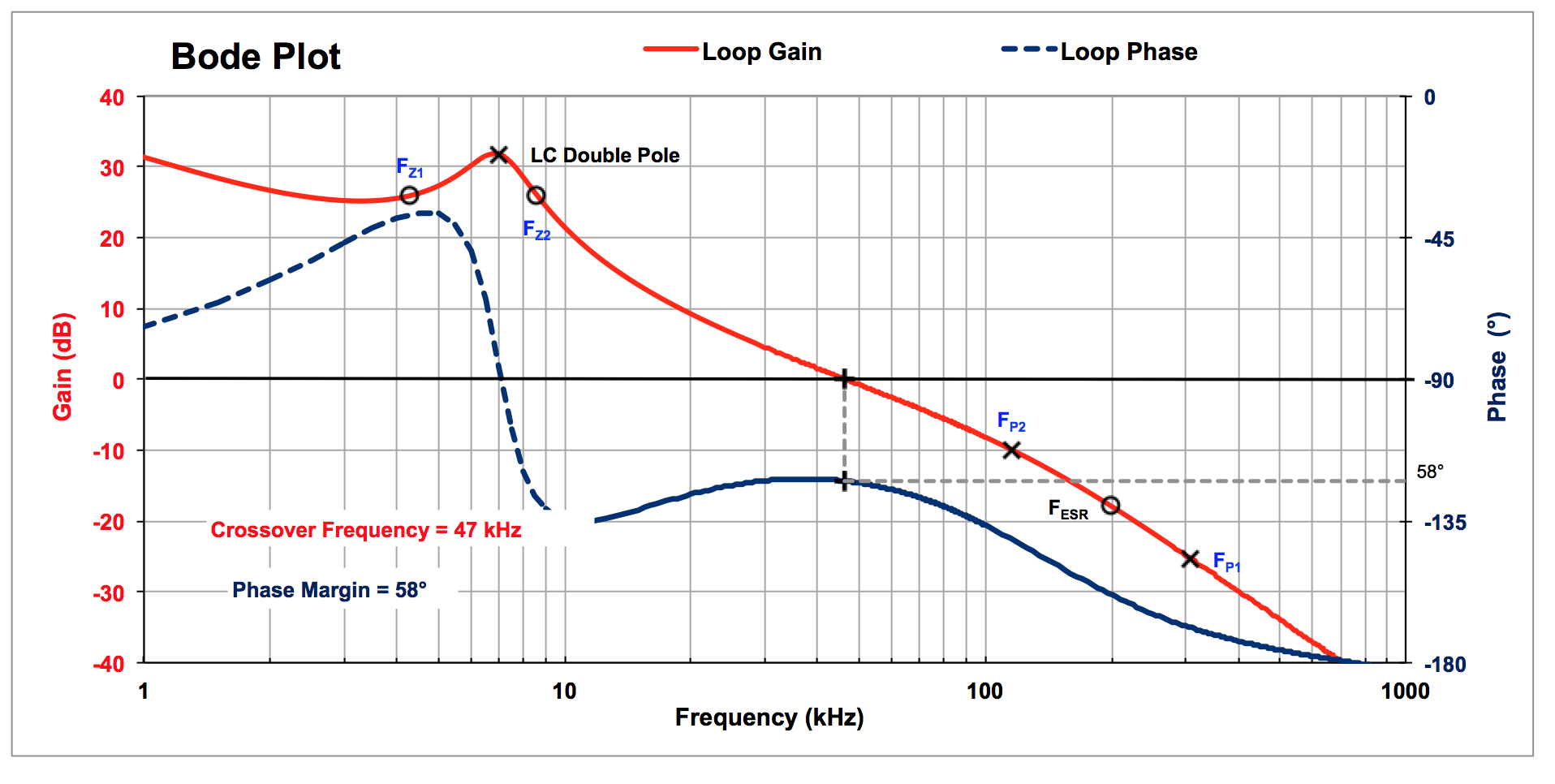
Some background, buck switches at 250khz with a 1.3uH inductor with 2.3mOhm DCR, and 400uF output caps with 2mOhm ESR.
I understand that increasing the crossover frequency will increase load transient performance, but at what cost? I also read that a properly designed zero and pole placement can help with attenuation of the high frequency noise (mine is at 83mhz @ 100mv).
Based on my values this is a Type III B compensator which says the second zero and first pole should be placed to get the maximum phase lead at the crossover frequency, and the first zero should be half the first zero, and that second pole placed at half the switching frequency.
Now the design tool for the LM27403 says that the first zero should be placed at the complex double pole frequency (Flc) which is 7khz for my setup, and the second zero at the Flc resonant frequency (which I'm not sure sure where that is exactly). Then the first pole at the ESR zero frequency of the output cap, and the second pole at half the switching frequency.
So im a little confused at which approach is "right" and which would have the best performance for my design needs of fast transient response and attenuating high frequency noise. Ive attached what my bode plot looks like when going with the first approach.
(where would the LC resonant frequency be on this plot?).