r1caw ex ua6bqg
Member level 2

Hi all!
I have a question related with the standard cell layout.
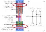
I have revised 28nm digital stdcells layout obtained from foundry and I am little bit confused - in this cells POLY layers (gates of MOS) are connected together in the upped and bottom parts of the cell (looks same as in the attached picture for the CMOS inverter).
Why they are connected together?


