Majid_Vatan_Parast
Junior Member level 3
Hello
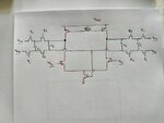
I want to design a capacitive common mode feedback , I have a circuit but it does not work .Can anyone tell me the problem of the circuit ?

I want to design a capacitive common mode feedback , I have a circuit but it does not work .Can anyone tell me the problem of the circuit ?