Continue to Site

Welcome to EDAboard.com

Welcome to our site! EDAboard.com is an international Electronics Discussion Forum focused on EDA software, circuits, schematics, books, theory, papers, asic, pld, 8051, DSP, Network, RF, Analog Design, PCB, Service Manuals... and a whole lot more! To participate you need to register. Registration is free. Click here to register now.

Clamping the input voltage to an IC?

Status
Not open for further replies.

cupoftea

Advanced Member level 5
Joined
Jun 13, 2021
Messages
2,611
Helped
54
Reputation
108
Reaction score
115
Trophy points
63
Activity points
13,685
Hi,
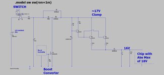
Have a 12V supply which will get suddenly switched into a connector…..where it will ring like billy-o with an input LC filter….there’s then a 12V to 16V Boost converter, and then a Gate Drive IC with 18V Abs Max. (The Gate drive IC will draw some 300mA, as its feeding a gate drive transformer)

The Abs Max is going to get violated so we need to interpose a ~17V clamp at the VCC input to the Gate Drive IC. We want it to dissipate as little as possible, and use as few components as poss…..can you think of a better way than the attached?

LTspice and jpeg schem attached
 

Attachments

  • Darlington voltage clamp.zip
    1 KB · Views: 92
  • Darlington voltage clamp.jpg
    Darlington voltage clamp.jpg
    123.9 KB · Views: 113

Hi,

I have not run the simulation, but what might ruin your day/IC is the specified zener diode voltage range at 25°C of 16.8 V up to 19.1 V. Further, high voltage zener diodes have a positive temperature coeficient, which might increase the actual zener voltage further. At the moment you are aiming to clamp a voltage difference of 1 V, and your reference might already vary by at least 1 V.

Also the silicon doide voltage drop will decrease at higher temperatures, which causes a higher “output“ voltage.

To me it looks like you have performed your analysis at the default temperature of 27°C.

BR
 
That isn't a clamp, its a series pass regulator. I'm supposing you really want the boost controller to produce 16V and the ringing is only present at time of powering on, before a settled state is reached so it will only last very briefly. I would consider a 17V Zener diode (1N5334 maybe) straight across the output or maybe with a small (1 Ohm) series resistor.

Brian.
 
I'm supposing you really want the boost controller to produce 16V and the ringing is only present at time of powering on, before a settled state is reached so it will only last very briefly.
Thanks, yes thats correct.

Also the silicon doide voltage drop will decrease at higher temperatures, which causes a higher “output“ voltage.
...since this is only one prototype, it should be OK to just check it and see....if it clamps to somewhere between 15.6V and 17.5V then ill be happy....i agree that a different batch of the zeners may be different.......but here ill just be using the one...thanks though.....as ill use a zero ohm link and check its ok before connecting up the IC.

I would consider a 17V Zener diode (1N5334 maybe) straight across the output or maybe with a small (1 Ohm) series resistor.
Thanks, this sounds like a solid solution, but ditto my above point (just one prototype , and ill check it before connecting)
 

The attached clamps the voltage to under x volts...and also regulates the voltage to y volts......any fewer component count solutions than this greatly appreciated

LTspice and jpeg attached.
 

Attachments

  • Voltage clamp.zip
    1.9 KB · Views: 113
  • Clamping to less than 7V___and regulating to 5V.jpg
    Clamping to less than 7V___and regulating to 5V.jpg
    116.5 KB · Views: 102

Thanks, with this one, its highly variable voltage output (change of divider res), and also can take higher vin than the lm780x range.
 

AD584 will take up to 40V supply and give a very accurate 2.5V output. that would eliminate everything before U1.
I can't see any purpose in R6/C6 as the voltage there should be steady, if you need to improve transient response I would do it in the output divider section instead of tailoring the op-amp feedback.
You can replace R9/R11/R12/R16/Q3/Q4/Q5/Q6 with a single darlington power transistor.
Suggestion: and I have not tried this, do all the above but also remove U1 and replace it with a long tailed pair, regulated 2.5V on one base and feedback on the other. It would do the inversion needed in the feedback path without needing any op-amps. You could even try single transistor with the 2.5V on the emitter, feedback on the base and drive to the darlington from the collector.

Brian.
 
This seems to have a lot of conjecture about Vcc rail goings-on below the surface. Particularly the boost converter, and the hot plug boundary. If the boost is hard connected to driver Vcc then hot plug may bounce the raw 12V but that has to make it past the output filter and may be nothing (unless boost DC-DC has unstable soft start overshoot). Or if your boost lacks SS and has too light a filter.

Seems to me you want to instrument up a unit and see what Vcc hot plug -really- induces, where it counts.
 
Status
Not open for further replies.

Similar threads

Part and Inventory Search

Welcome to EDABoard.com

Sponsor

Back
Top